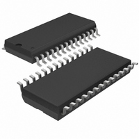
LTC1415CSW#TRPBF Linear Technology, LTC1415CSW#TRPBF Datasheet - Page 12

LTC1415CSW#TRPBF
Manufacturer Part Number
LTC1415CSW#TRPBF
Description
IC A/D CONV 12BIT SAMPLNG 28SOIC
Manufacturer
Linear Technology
Datasheet
1.LTC1415CSWPBF.pdf
(24 pages)
Specifications of LTC1415CSW#TRPBF
Number Of Bits
12
Sampling Rate (per Second)
1.25M
Data Interface
Parallel
Number Of Converters
1
Power Dissipation (max)
100mW
Voltage Supply Source
Single Supply
Operating Temperature
0°C ~ 70°C
Mounting Type
Surface Mount
Package / Case
28-SOIC (0.300", 7.50mm Width)
Lead Free Status / RoHS Status
Lead free / RoHS Compliant
Available stocks
Company
Part Number
Manufacturer
Quantity
Price
LTC1415
circuitry. The reference amplifier gains the voltage at the
V
voltage of 4.096V. This provides buffering between the
V
amplifier compensation pin (REFCOMP, Pin 4) must be
bypassed with a capacitor to ground. The reference ampli-
fier is stable with capacitors of 1 F or greater. For the best
noise performance a 10 F ceramic or tantalum in parallel
with a 0.1 F ceramic is recommended.
The V
shown in Figure 9. This is useful in applications where the
peak input signal amplitude may vary. The input span of
the ADC can then be adjusted to match the peak input
signal, maximizing the signal-to-noise ratio. The filtering
of the internal LTC1415 reference amplifier will limit the
12
APPLICATIONS
REF
REF
4.096V
Figure 8b. Using the LT1019-2.5 as an External Reference
pin and the high speed capacitive DAC. The reference
pin by 1.638 to create the required internal reference
REF
2.500V
LT1019A-2.5
pin can be driven with a DAC or other means
10 F
V
5V
IN
Figure 8a. LTC1415 Reference Circuit
3
4
5
V
OUT
V
REFCOMP
AGND
REF
ANALOG
U
64k
INPUT
R3
REFERENCE
40k
R2
10 F
AMP
INFORMATION
U
1
2
3
4
5
+A
–A
V
REFCOMP
AGND
REF
IN
IN
R1
2k
LTC1415
W
REFERENCE
BANDGAP
LTC1415
LTC1415 • F08a
1415 F08b
U
bandwidth and settling time of this circuit. A settling time
of 5ms should be allowed for after a reference adjustment.
Differential Inputs
The LTC1415 has a unique differential sample-and-hold
circuit that allows rail-to-rail inputs. The ADC will always
convert the difference of +A
common mode voltage. The common mode rejection is
constant from DC to 1MHz, see Figure 10a. The only
requirement is that both inputs can not exceed the AV
or AGND power supply voltages. Integral nonlinearity
errors (INL) and differential nonlinearity errors (DNL) are
independent of the common mode voltage, however, the
bipolar zero error (BZE) will vary. The change in BZE is
typically less than 0.1% of the common mode voltage.
Differential inputs allow greater flexibility for accepting
different input ranges. Figure 10b shows a circuit that
shifts the input range up in voltage by 200mV. This can be
useful in applications where the amplifier driving the ADC
input is not able to swing all the way to ground, because
of output loading or settling time issues.
Some AC applications may have their performance limited
by distortion. Most circuits exhibit higher distortion when
signals approach the supply or ground. Distortion can be
reduced by reducing the signal amplitude and keeping the
common mode voltage at approximately midsupply. The
circuit of Figure 10c reduces the ADC full scale from
Figure 9. Driving V
RAIL-TO-RAIL DAC
LTC1450
12-BIT
DIFFERENTIAL ANALOG INPUT
RANGE = (V
REF
1.25V TO 3V
REF
with a DAC to Adjust Full Scale
)(1.638)
IN
10 F
– (–A
1
2
3
4
5
IN
+A
–A
V
REFCOMP
AGND
REF
) independent of the
IN
IN
LTC1415
LTC1415 • F09
DD


