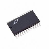
LTC1272-3CCSW#PBF Linear Technology, LTC1272-3CCSW#PBF Datasheet - Page 3

LTC1272-3CCSW#PBF
Manufacturer Part Number
LTC1272-3CCSW#PBF
Description
IC A/D CONV 12BIT SAMPLNG 24SOIC
Manufacturer
Linear Technology
Datasheet
1.LTC1272-3CCSW.pdf
(20 pages)
Specifications of LTC1272-3CCSW#PBF
Number Of Bits
12
Sampling Rate (per Second)
250k
Data Interface
Parallel
Number Of Converters
1
Power Dissipation (max)
75mW
Voltage Supply Source
Single Supply
Operating Temperature
0°C ~ 70°C
Mounting Type
Surface Mount
Package / Case
24-SOIC (0.300", 7.50mm Width)
Lead Free Status / RoHS Status
Lead free / RoHS Compliant
Available stocks
Company
Part Number
Manufacturer
Quantity
Price
I TER AL REFERE CE CHARACTERISTICS
DIGITAL AND DC ELECTRICAL CHARACTERISTICS
DY
A
operating temperature range, otherwise specifications are at T
PARAMETER
V
V
V
V
apply over the full operating temperature range, otherwise specifications are at T
SYMBOL
V
V
I
V
V
I
C
I
I
I
P
specifications are at T
SYMBOL
V
I
C
t
SYMBOL
S/(N + D)
THD
IN
OZ
SOURCE
SINK
DD
IN
ACQ
U
REF
REF
REF
REF
IH
IL
OH
OL
OZ
D
IN
IN
U
Output Voltage (Note 6)
Output Tempco
Line Regulation
Load Regulation (Sourcing Current) 0 ≤ ⎢I
U W
A
A
LOG
U
PARAMETER
Input Voltage Range
Input Current
Input Capacitance
Sample-and-Hold Acquisition Time
PARAMETER
High Level Input Voltage CS, RD, HBEN, CLK IN
Low Level Input Voltage CS, RD, HBEN, CLK IN
Input Current CS, RD, HBEN
Input Current CLK IN
High Level Output Voltage All Logic Outputs
Low Level Output Voltage All Logic Outputs
High-Z Output Leakage D11-D0/8
High-Z Output Capacitance (Note 7)
Output Source Current
Output Sink Current
Positive Supply Current
Power Dissipation
PARAMETER
Signal-to-Noise Plus Distortion Ratio
Total Harmonic Distortion (Up to 5th Harmonic)
Peak Harmonic or Spurious Noise
IC
I
U
ACCURACY
U
A
PUT
= 25°C. (Note 4)
U
The
CONDITIONS
I
I
4.75V ≤ V
OUT
OUT
●
denotes the specifications which apply over the full operating temperature range, otherwise
(Note 4) f
= 0
= 0
OUT
⎢ ≤ 1mA
DD
≤ 5.25V, I
SAMPLE
OUT
= 250kHz (LTC1272-3), 166kHz (LTC1272-5), 111kHz (LTC1272-8)
= 0
CONDITIONS
V
V
V
V
V
V
V
V
V
CS = RD = V
CONDITIONS
4.75V ≤ V
CONDITIONS
10kHz Input Signal
10kHz Input Signal
10kHz Input Signal
A
DD
DD
IN
IN
DD
DD
OUT
OUT
OUT
= 25°C. (Note 4)
= 0V to V
= 0V to V
= 5.25V
= 4.75V
= 4.75V
= 4.75V, I
= 0V to V
= 0V
= V
●
DD
DD
2.400
DD
MIN
≤ 5.25V
DD
DD
OUT
DD
, A
I
The
I
OUT
OUT
IN
= 1.6mA
LTC1272-XA
= 5V
= – 200µA
= – 10µA
●
A
2.420
denotes the specifications which apply over the full
0.01
TYP
= 25°C. (Note 4)
5
2
The
2.440
MAX
25
●
●
●
●
●
●
●
●
●
●
●
●
●
denotes the specifications which
2.400
MIN
MIN
MIN
MIN
2.4
0
LTC1272-XA/B/C
LTC1272-XA/C
LTC1272-XA/C
LTC1272-XC
2.420
0.01
0.45
TYP
TYP
TYP
– 82
– 82
TYP
– 10
50
10
4.7
4.0
72
10
15
75
2
LTC1272
2.440
MAX
MAX
MAX
±10
±20
±10
MAX
0.8
0.4
15
30
3.5
45
5
1
LSB/mA
ppm/°C
UNITS
UNITS
UNITS
UNITS
LSB/V
1272fb
3
mW
mA
mA
mA
mA
µA
µA
µA
dB
dB
dB
µs
pF
pF
V
V
V
V
V
V
V


