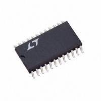
LTC1272-3CCSW#TR Linear Technology, LTC1272-3CCSW#TR Datasheet - Page 18

LTC1272-3CCSW#TR
Manufacturer Part Number
LTC1272-3CCSW#TR
Description
IC ADC 12BIT SAMPLING 24SOIC
Manufacturer
Linear Technology
Datasheet
1.LTC1272-3CCSW.pdf
(20 pages)
Specifications of LTC1272-3CCSW#TR
Number Of Bits
12
Sampling Rate (per Second)
250k
Data Interface
Parallel
Number Of Converters
1
Power Dissipation (max)
75mW
Voltage Supply Source
Single Supply
Operating Temperature
0°C ~ 70°C
Mounting Type
Surface Mount
Package / Case
24-SOIC (0.300", 7.50mm Width)
Lead Free Status / RoHS Status
Contains lead / RoHS non-compliant
Available stocks
Company
Part Number
Manufacturer
Quantity
Price
A
LTC1272
18
If the clock signal for the AD7572 is derived from a
separate crystal or other signal which is not synchronous
with the microprocessor clock, then the signals need to be
synchronized for the LTC1272 to achieve best analog
performance (see Clock and Control Synchronization).
The best way to synchronize these signals is to drive the
CLK IN pin of the LTC1272 with a derivative of the
processor clock, as mentioned above and shown in Figure
22. Another way, shown in Figure 23, is to use a flip-flop
to synchronize the RD to the LTC1272 with the CLK IN
signal. This method will work but has two disavantages
PPLICATI
OUTPUT
2.42V
V
REF
*
+
ANALOG INPUT
10µF
O
(0V TO 5V)
U
S
DATA
0.1µF
BUS
µ
I FOR ATIO
P
U
10 Ω
*
Figure 22. Plugging the LTC1272 into an AD7572 Socket
Case 1: Clock Synchronous with CS and RD
W
D11 (MSB)
D10
D9
D8
D7
D6
D5
D4
A
V
AGND
DGND
REF
IN
LTC1272
CLK IN**
CLK OUT
D2/10
BUSY
HBEN
D3/11
D0/8
D1/9
NC
V
RD
CS
DD
✝
U
µ
CONTROL
LINES
P
**
*
✝
THE LTC1272 HAS THE SAME 0V TO 5V INPUT RANGE BUT PROVIDES A 2.42V
REFERENCE OUTPUT AS OPPOSED TO THE –5.25V OF THE AD7572. FOR PROPER
OPERATION, REVERSE THE REFERENCE CAPACITOR POLARITY AND SHORT OUT THE
10 RESISTOR.
THE ADC CLOCK SHOULD BE SYNCHRONIZED TO THE CONVERSION START
SIGNALS (CS, RD) OR 1-2 LSBs OF OUTPUT CODE NOISE MAY OCCUR. DERIVING
THE ADC CLOCK FROM THE P CLOCK IS ADEQUATE.
THE LTC1272 CAN ACCOMMODATE THE –15V SUPPLY OF THE AD7572 BUT DOES
NOT REQUIRE IT. PIN 23 OF THE LTC1272 IS NOT INTERNALLY CONNECTED.
over the first: because the RD is delayed by the flip-flop,
the actual conversion start and the enabling of the
LTC1272’s BUSY and data outputs can take up to one CLK
IN cycle to respond to a RD↓ convert command from the
processor. The sampling of the analog input no longer
occurs at the processor’s falling RD edge but may be
delayed as much as one CLK IN cycle. Although the
LTC1272 will still exhibit excellent DC performance, the
flip-flop will introduce jitter into the sampling which may
reduce the usefulness of this method for AC systems.
Ω
0.1 F
µ
+
10 F
–15V
µ
µ
†
0.1 F
µ
+
10 F
5V
µ
LTC1272 • TA04
1272fb
1272fb
1272fb


