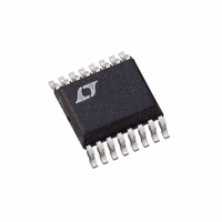
LTC1867AIGN#TRPBF Linear Technology, LTC1867AIGN#TRPBF Datasheet - Page 4

LTC1867AIGN#TRPBF
Manufacturer Part Number
LTC1867AIGN#TRPBF
Description
IC ADC 16BIT 8CH 200KSPS 16SSOP
Manufacturer
Linear Technology
Datasheet
1.LTC1867CGNPBF.pdf
(16 pages)
Specifications of LTC1867AIGN#TRPBF
Number Of Bits
16
Sampling Rate (per Second)
200k
Data Interface
MICROWIRE™, Serial, SPI™
Number Of Converters
1
Power Dissipation (max)
9mW
Voltage Supply Source
Single Supply
Operating Temperature
-40°C ~ 85°C
Mounting Type
Surface Mount
Package / Case
16-SSOP (0.150", 3.90mm Width)
Lead Free Status / RoHS Status
Lead free / RoHS Compliant
Available stocks
Company
Part Number
Manufacturer
Quantity
Price
LTC1863/LTC1867
DIGITAL INPUTS AND DIGITAL OUTPUTS
full operating temperature range, otherwise specifi cations are at T
SYMBOL
C
V
V
I
I
POWER REQUIREMENTS
range, otherwise specifi cations are at T
SYMBOL
V
I
P
TIMING CHARACTERISTICS
range, otherwise specifi cations are at T
SYMBOL
f
t
t
f
t
t
t
t
t
t
t
t
Note 1: Stresses beyond those listed under Absolute Maximum Ratings
may cause permanent damage to the device. Exposure to any Absolute
Maximum Rating condition for extended periods may affect device
reliability and lifetime
4
SOURCE
SINK
DD
SAMPLE
SCK
1
4
5
7
8
CONV
ACQ
2
3
6
IN
OH
OL
DD
DISS
PARAMETER
Digital Input Capacitance
High Level Output Voltage (SDO)
Low Level Output Voltage (SDO)
Output Source Current
Output Sink Current
Hi-Z Output Leakage
Hi-Z Output Capacitance
Data Format
PARAMETER
Supply Voltage
Supply Current
Power Dissipation
PARAMETER
Maximum Sampling Frequency
Conversion Time
Acquisition Time
SCK Frequency
CS/CONV High Time
SDO Valid After SCK↓
SDO Valid Hold Time After SCK↓
SDO Valid After CS/CONV↓
SDI Setup Time Before SCK↑
SDI Hold Time After SCK↑
SLEEP Mode Wake-Up Time
Bus Relinquish Time After CS/CONV↑
A
A
= 25°C. (Note 5)
= 25°C. (Note 5)
The
CONDITIONS
V
V
V
V
SDO = 0V
SDO = V
CS/CONV = High, SDO = 0V or V
CS/CONV = High (Note 10)
Unipolar
Bipolar
CONDITIONS
(Note 9)
f
NAP Mode
SLEEP Mode
CONDITIONS
Short CS/CONV Pulse Mode
C
C
C
C
C
SAMPLE
L
L
L
REFCOMP
L
DD
DD
DD
DD
= 25pF (Note 11)
= 25pF
= 25pF
= 25pF
The
l
= 4.75V, I
= 4.75V, I
= 4.75V, I
= 4.75V, I
denotes the specifi cations which apply over the full operating temperature
l
DD
= 200ksps
denotes the specifi cations which apply over the full operating temperature
= 10μF, C
O
O
O
O
= –10μA
= –200μA
= 160μA
= 1.6mA
A
VREF
= 25°C. (Note 5)
Note 2: All voltage values are with respect to GND (unless otherwise noted).
Note 3: When these pin voltages are taken below GND or above V
will be clamped by internal diodes. This product can handle input currents
of greater than 100mA without latchup.
= 2.2μF
The
DD
l
denotes the specifi cations which apply over the
l
l
l
l
l
l
l
l
l
l
l
l
l
l
l
l
l
LTC1863/LTC1867/LTC1867A
LTC1863/LTC1867/LTC1867A
LTC1863/LTC1867/LTC1867A
MIN
MIN
4.75
MIN
200
1.5
40
15
10
4
5
Two’s Complement
Straight Binary
TYP
4.75
4.74
0.05
TYP
TYP
–32
150
100
0.2
6.5
0.1
1.3
1.1
19
13
11
10
–6
60
20
2
3
4
MAX
MAX
MAX
5.25
±10
0.4
3.5
1.8
15
40
22
30
40
3
9
DD
, they
UNITS
UNITS
UNITS
18637fa
MHz
mW
kHz
mA
mA
mA
ms
μA
μA
pF
μA
μs
μs
ns
ns
ns
ns
ns
ns
ns
pF
V
V
V
V
V


