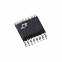
LTC1867AIGN#TRPBF Linear Technology, LTC1867AIGN#TRPBF Datasheet - Page 7

LTC1867AIGN#TRPBF
Manufacturer Part Number
LTC1867AIGN#TRPBF
Description
IC ADC 16BIT 8CH 200KSPS 16SSOP
Manufacturer
Linear Technology
Datasheet
1.LTC1867CGNPBF.pdf
(16 pages)
Specifications of LTC1867AIGN#TRPBF
Number Of Bits
16
Sampling Rate (per Second)
200k
Data Interface
MICROWIRE™, Serial, SPI™
Number Of Converters
1
Power Dissipation (max)
9mW
Voltage Supply Source
Single Supply
Operating Temperature
-40°C ~ 85°C
Mounting Type
Surface Mount
Package / Case
16-SSOP (0.150", 3.90mm Width)
Lead Free Status / RoHS Status
Lead free / RoHS Compliant
Available stocks
Company
Part Number
Manufacturer
Quantity
Price
PIN FUNCTIONS
CHO-CH7/COM (Pins 1-8): Analog Input Pins. Analog
inputs must be free of noise with respect to GND. CH7/COM
can be either a separate channel or the common minus
input for the other channels.
REFCOMP (Pin 9): Reference Buffer Output Pin. Bypass
to GND with 10μF tantalum capacitor in parallel with
0.1μF ceramic capacitor (4.096V Nominal). To overdrive
REFCOMP, tie V
V
be used as an external reference buffer input for improved
accuracy and drift. Bypass to GND with 2.2μF tantalum
capacitor in parallel with 0.1μF ceramic capacitor.
CS/CONV (Pin 11): This input provides the dual function
of initiating conversions on the ADC and also frames the
serial data transfer.
TYPICAL CONNECTION DIAGRAM
TEST CIRCUITS
REF
(Pin 10): 2.5V Reference Output. This pin can also
(A) Hi-Z TO V OH AND V OL TO V OH
DN
Load Circuits for Access Timing
REF
3k
to GND.
C
L
(B) Hi-Z TO V OL AND V OH TO V OL
SINGLE-ENDED
DIFFERENTIAL
DN
±2.048V
INPUTS
4.096V
INPUT
5V
–
+
+
3k
C
L
CH0
CH1
CH2
CH3
CH4
CH5
CH6
CH7/COM
18637 TC01
LTC1863/
LTC1867
REFCOMP
CS/CONV
V
GND
SDO
SCK
SCK (Pin 12): Shift Clock. This clock synchronizes the
serial data transfer.
SDO (Pin 13): Digital Data Output. The A/D conversion
result is shifted out of this output. Straight binary format
for unipolar mode and two’s complement format for
bipolar mode.
SDI (Pin 14): Digital Data Input Pin. The A/D confi guration
word is shifted into this input.
GND (Pin 15): Analog and Digital GND.
V
GND with 10μF tantalum capacitor in parallel with 0.1μF
ceramic capacitor.
V
SDI
REF
DD
DD
(Pin 16): Analog and Digital Power Supply. Bypass to
DIGITAL
I/O
10μF
DN
4.096V
5V
Load Circuits for Output Float Delay
(A) V OH TO Hi-Z
3k
LTC1863/LTC1867
18637 TCD
2.2μF
2.5V
C
L
DN
(B) V OL TO Hi-Z
5V
3k
18637 TC02
C
L
18637fa
7


