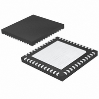
LTC2224CUK Linear Technology, LTC2224CUK Datasheet - Page 18

LTC2224CUK
Manufacturer Part Number
LTC2224CUK
Description
IC ADC 12BIT 135MSPS SAMPL 48QFN
Manufacturer
Linear Technology
Datasheet
1.LTC2224CUKPBF.pdf
(24 pages)
Specifications of LTC2224CUK
Number Of Bits
12
Sampling Rate (per Second)
135M
Data Interface
Parallel
Number Of Converters
1
Power Dissipation (max)
680mW
Voltage Supply Source
Single Supply
Operating Temperature
0°C ~ 70°C
Mounting Type
Surface Mount
Package / Case
48-WFQFN, Exposed Pad
Lead Free Status / RoHS Status
Contains lead / RoHS non-compliant
Available stocks
Company
Part Number
Manufacturer
Quantity
Price
Part Number:
LTC2224CUK
Manufacturer:
LTNEAR
Quantity:
20 000
APPLICATIO S I FOR ATIO
LTC2224
DIGITAL OUTPUTS
Table 1 shows the relationship between the analog input
voltage, the digital data bits and the overflow bit.
Table 1. Output Codes vs Input Voltage
Digital Output Buffers
Figure 13 shows an equivalent circuit for a single output
buffer. Each buffer is powered by OV
are isolated from the ADC power and ground. The addi-
tional N-channel transistor in the output driver allows
operation down to voltages as low as 0.5V. The internal
resistor in series with the output makes the output appear
as 50Ω to external circuitry and may eliminate the need for
external damping resistors.
18
>+1.000000V
<–1.000000V
A
(2V Range)
+0.999512V
+0.999024V
+0.000488V
–0.000488V
–0.000976V
–0.999512V
–1.000000V
0.000000V
IN
Figure 12b. ENC Drive Using a CMOS to PECL Translator
+
– A
IN
–
V
THRESHOLD
MC100LVELT22
Figure 12a. Single-Ended ENC Drive,
Not Recommended for Low Jitter
OF
1
0
0
0
0
0
0
0
0
1
= 1.6V
U
D0
1111 1111 1111
1111 1111 1111
1111 1111 1110
1000 0000 0001
1000 0000 0000
0111 1111 1111
0111 1111 1110
0000 0000 0001
0000 0000 0000
0000 0000 0000
(Offset Binary)
3.3V
0.1µF
D11 – D0
U
Q0
Q0
130Ω
1.6V
83Ω
ENC
ENC
3.3V
W
+
–
DD
LTC2224
ENC
ENC
130Ω
83Ω
and OGND, which
(2’s Complement)
+
–
0111 1111 1111
0111 1111 1111
0111 1111 1110
0000 0000 0001
0000 0000 0000
1111 1111 1111
1111 1111 1110
1000 0000 0001
1000 0000 0000
1000 0000 0000
2224 F12a
D11 – D0
LTC2224
U
2224 F12b
As with all high speed/high resolution converters, the
digital output loading can affect the performance. The
digital outputs of the LTC2224 should drive a minimal
capacitive load to avoid possible interaction between the
digital outputs and sensitive input circuitry. For full speed
operation the capacitive load should be kept under 5pF.
Lower OV
from the digital outputs and improve the SNR.
Data Format
The LTC2224 parallel digital output can be selected for
offset binary or 2’s complement format. The format is
selected with the MODE pin. Connecting MODE to GND or
1/3V
MODE to 2/3V
format. An external resistor divider can be used to set the
1/3V
states for the MODE pin.
Table 2. MODE Pin Function
MODE Pin
0
1/3V
2/3V
V
LATCH
FROM
DD
DATA
OE
DD
DD
DD
DD
PREDRIVER
or 2/3V
selects offset binary output format. Connecting
LOGIC
DD
V
DD
voltages will also help reduce interference
DD
Figure 13. Digital Output Buffer
2’s Complement
2’s Complement
DD
Output Format
Offset Binary
Offset Binary
or V
logic values. Table 2 shows the logic
DD
selects 2’s complement output
V
DD
OV
Cycle Stablizer
DD
Clock Duty
LTC2224
Off
On
On
Off
43Ω
2224 F13
OV
OGND
DD
TYPICAL
DATA
OUTPUT
0.5V
TO 3.6V
0.1µF
2224fa


