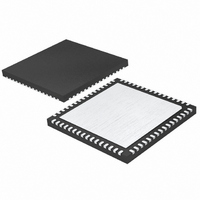
LTC2240CUP-12#TRPBF Linear Technology, LTC2240CUP-12#TRPBF Datasheet - Page 9

LTC2240CUP-12#TRPBF
Manufacturer Part Number
LTC2240CUP-12#TRPBF
Description
IC ADC 12BIT 170MSPS 64-QFN
Manufacturer
Linear Technology
Datasheet
1.LTC2240CUP-12PBF.pdf
(28 pages)
Specifications of LTC2240CUP-12#TRPBF
Number Of Bits
12
Sampling Rate (per Second)
170M
Data Interface
Parallel
Number Of Converters
1
Power Dissipation (max)
638mW
Voltage Supply Source
Single Supply
Operating Temperature
0°C ~ 70°C
Mounting Type
Surface Mount
Package / Case
64-WFQFN, Exposed Pad
Lead Free Status / RoHS Status
Lead free / RoHS Compliant
Available stocks
Company
Part Number
Manufacturer
Quantity
Price
PIN FUNCTIONS
(CMOS Mode)
A
A
REFHA (Pins 5, 6): ADC High Reference. Bypass to
Pins 7, 8 with 0.1μF ceramic chip capacitor, to Pins 11,
12 with a 2.2μF ceramic capacitor and to ground with 1μF
ceramic capacitor.
REFLB (Pins 7, 8): ADC Low Reference. Bypass to Pins
5, 6 with 0.1μF ceramic chip capacitor. Do not connect to
Pins 11, 12.
REFHB (Pins 9, 10): ADC High Reference. Bypass to
Pins 11, 12 with 0.1μF ceramic chip capacitor. Do not
connect to Pins 5, 6.
REFLA (Pins 11, 12): ADC Low Reference. Bypass to
Pins 9, 10 with 0.1μF ceramic chip capacitor, to Pins 5,
6 with a 2.2μF ceramic capacitor and to ground with 1μF
ceramic capacitor.
V
GND with 0.1μF ceramic chip capacitors.
GND (Pins 16, 61, 64): ADC Power Ground.
ENC
positive edge.
ENC
starts on the negative edge. Bypass to ground with 0.1μF
ceramic for single-ended encode signal.
SHDN (Pin 19): Shutdown Mode Selection Pin. Connecting
SHDN to GND and OE to GND results in normal operation
with the outputs enabled. Connecting SHDN to GND and
OE to V
high impedance. Connecting SHDN to V
results in nap mode with the outputs at high impedance.
Connecting SHDN to V
mode with the outputs at high impedance.
OE (Pin 20): Output Enable Pin. Refer to SHDN pin func-
tion.
DB0 - DB11 (Pins 21, 22, 23, 24, 27, 28, 29, 30, 31,
32, 35, 36): Digital Outputs, B Bus. DB11 is the MSB. At
high impedance in full rate CMOS mode.
OGND (Pins 25, 33, 41, 50): Output Driver Ground.
OV
Output Drivers. Bypass to ground with 0.1μF ceramic chip
capacitor.
IN
IN
DD
DD
+
–
+
–
(Pins 13, 14, 15, 62, 63): 2.5V Supply. Bypass to
(Pins 1, 2): Positive Differential Analog Input.
(Pins 3, 4): Negative Differential Analog Input.
(Pin 17): Encode Input. Conversion starts on the
(Pin 18): Encode Complement Input. Conversion
(Pins 26, 34, 42, 49): Positive Supply for the
DD
results in normal operation with the outputs at
DD
and OE to V
DD
DD
results in sleep
and OE to GND
OFB (Pin 37): Over/Under Flow Output for B Bus. High
when an over or under fl ow has occurred. At high imped-
ance in full rate CMOS mode.
CLKOUTB (Pin 38): Data Valid Output for B Bus. In demux
mode with interleaved update, latch B bus data on the fall-
ing edge of CLKOUTB. In demux mode with simultaneous
update, latch B bus data on the rising edge of CLKOUTB.
This pin does not become high impedance in full rate
CMOS mode.
CLKOUTA (Pin 39): Data Valid Output for A Bus. Latch A
bus data on the falling edge of CLKOUTA.
DA0 - DA11 (Pins 40, 43, 44, 45, 46, 47, 48, 51, 52, 53,
54, 55): Digital Outputs, A Bus. DA11 is the MSB.
OFA (Pin 56): Over/Under Flow Output for A Bus. High
when an over or under fl ow has occurred.
LVDS (Pin 57): Output Mode Selection Pin. Connecting
LVDS to 0V selects full rate CMOS mode. Connecting LVDS
to 1/3V
update. Connecting LVDS to 2/3V
mode with interleaved update. Connecting LVDS to V
selects LVDS mode.
MODE (Pin 58): Output Format and Clock Duty Cycle
Stabilizer Selection Pin. Connecting MODE to 0V selects
offset binary output format and turns the clock duty cycle
stabilizer off. Connecting MODE to 1/3V
binary output format and turns the clock duty cycle stabilizer
on. Connecting MODE to 2/3V
output format and turns the clock duty cycle stabilizer on.
Connecting MODE to V
format and turns the clock duty cycle stabilizer off.
SENSE (Pin 59): Reference Programming Pin. Connecting
SENSE to V
input range. Connecting SENSE to V
reference and a ±1V input range. An external reference
greater than 0.5V and less than 1V applied to SENSE
selects an input range of ±V
input range.
V
Bypass to ground with 2.2μF ceramic chip capacitor.
GND (Exposed Pad) (Pin 65): ADC Power Ground. The
exposed pad on the bottom of the package needs to be
soldered to ground.
CM
(Pin 60): 1.25V Output and Input Common Mode Bias.
DD
selects demux CMOS mode with simultaneous
CM
selects the internal reference and a ±0.5V
DD
selects 2’s complement output
SENSE
DD
DD
LTC2240-12
selects 2’s complement
. ±1V is the largest valid
DD
selects demux CMOS
selects the internal
DD
selects offset
224012fc
9
DD


