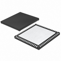
LTC2240IUP-12#TRPBF Linear Technology, LTC2240IUP-12#TRPBF Datasheet - Page 23

LTC2240IUP-12#TRPBF
Manufacturer Part Number
LTC2240IUP-12#TRPBF
Description
IC ADC 12BIT 170MSPS 64-QFN
Manufacturer
Linear Technology
Datasheet
1.LTC2240CUP-12PBF.pdf
(28 pages)
Specifications of LTC2240IUP-12#TRPBF
Number Of Bits
12
Sampling Rate (per Second)
170M
Data Interface
Parallel
Number Of Converters
1
Power Dissipation (max)
638mW
Voltage Supply Source
Single Supply
Operating Temperature
-40°C ~ 85°C
Mounting Type
Surface Mount
Package / Case
64-WFQFN, Exposed Pad
Lead Free Status / RoHS Status
Lead free / RoHS Compliant
Available stocks
Company
Part Number
Manufacturer
Quantity
Price
APPLICATIONS INFORMATION
some source termination to reduce ringing that may occur
even over a fraction of an inch is advisable. You must not
allow the clock to overshoot the supplies or performance
will suffer. Do not fi lter the clock signal with a narrow band
fi lter unless you have a sinusoidal clock source, as the
rise and fall time artifacts present in typical digital clock
signals will be translated into phase noise.
The lowest phase noise oscillators have single-ended
sinusoidal outputs, and for these devices the use of a
fi lter close to the ADC may be benefi cial. This fi lter should
be close to the ADC to both reduce roundtrip refl ection
times, as well as reduce the susceptibility of the traces
between the fi lter and the ADC. If the circuit is sensitive
to close-in phase noise, the power supply for oscillators
and any buffers must be very stable, or propagation de-
lay variation with supply will translate into phase noise.
Even though these clock sources may be regarded as
digital devices, do not operate them on a digital supply.
If your clock is also used to drive digital devices such as
an FPGA, you should locate the oscillator, and any clock
fan-out devices close to the ADC, and give the routing
to the ADC precedence. The clock signals to the FPGA
should have series termination at the driver to prevent
high frequency noise from the FPGA disturbing the sub-
strate of the clock fan-out device. If you use an FPGA as a
programmable divider, you must re-time the signal using
the original oscillator, and the re-timing fl ip-fl op as well
as the oscillator should be close to the ADC, and powered
with a very quiet supply.
For cases where there are multiple ADCs, or where the
clock source originates some distance away, differential
clock distribution is advisable. This is advisable both from
the perspective of EMI, but also to avoid receiving noise
from digital sources both radiated, as well as propagated in
the waveguides that exist between the layers of multilayer
PCBs. The differential pairs must be close together and
distanced from other signals. The differential pair should
be guarded on both sides with copper distanced at least
3x the distance between the traces, and grounded with
vias no more than 1/4 inch apart.
LTC2240-12
23
224012fc


