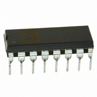
AD7715ANZ-3 Analog Devices Inc, AD7715ANZ-3 Datasheet - Page 12

AD7715ANZ-3
Manufacturer Part Number
AD7715ANZ-3
Description
IC ADC 16BIT SIGMA-DELTA 16DIP
Manufacturer
Analog Devices Inc
Specifications of AD7715ANZ-3
Data Interface
DSP, MICROWIRE™, QSPI™, Serial, SPI™
Number Of Bits
16
Sampling Rate (per Second)
500
Number Of Converters
1
Power Dissipation (max)
9.5mW
Voltage Supply Source
Analog and Digital
Operating Temperature
-40°C ~ 85°C
Mounting Type
Through Hole
Package / Case
16-DIP (0.300", 7.62mm)
Resolution (bits)
16bit
Input Channel Type
Differential
Supply Voltage Range - Analogue
3V To 3.6V
Supply Voltage Range - Digital
3V To 5.25V
Supply Current
600µA
No. Of
RoHS Compliant
Sampling Rate
19.2kSPS
Rohs Compliant
Yes
Lead Free Status / RoHS Status
Lead free / RoHS Compliant
For Use With
EVAL-AD7715-3EBZ - BOARD EVALUATION FOR AD7715
Lead Free Status / RoHS Status
Lead free / RoHS Compliant
Available stocks
Company
Part Number
Manufacturer
Quantity
Price
Company:
Part Number:
AD7715ANZ-3
Manufacturer:
INFINEON
Quantity:
12
Part Number:
AD7715ANZ-3
Manufacturer:
ADI/亚德诺
Quantity:
20 000
AD7715
ON-CHIP REGISTERS
The AD7715 contains four on-chip registers, which can be
accessed by via the serial port on the part. The first of these
is a communications register that decides whether the next
operation is a read or write operation and also decides which
register the read or write operation accesses. All communi-
cations to the part must start with a write operation to the
communications register. After power-on or RESET, the
device expects a write to its communications register. The data
written to this register determines whether the next operation
to the part is a write or a read operation and also determines to
which register this read or write operation occurs. Therefore,
write access to any of the other registers on the part starts with
a write operation to the communications register followed by a
write to the selected register. A read operation from any register
on the part (including the communications register itself and
Rev. D | Page 12 of 40
the output data register) starts with a write operation to the
communications register followed by a read operation from the
selected register. The communication register also controls the
standby mode and the operating gain of the part. The DRDY status
is also available by reading from the communications register. The
second register is a setup register that determines calibration
modes, filter selection and bipolar/unipolar operation. The
third register is the data register from which the output data
from the part is accessed. The final register is a test register
that is accessed when testing the device. It is advised that the
user does not attempt to access or change the contents of the
test register as it may lead to unspecified operation of the
device. The registers are discussed in more detail in the
following sections.


