AD7715ANZ-3 Analog Devices Inc, AD7715ANZ-3 Datasheet - Page 4
AD7715ANZ-3
Manufacturer Part Number
AD7715ANZ-3
Description
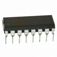
IC ADC 16BIT SIGMA-DELTA 16DIP
Manufacturer
Analog Devices Inc
Specifications of AD7715ANZ-3
Data Interface
DSP, MICROWIRE™, QSPI™, Serial, SPI™
Number Of Bits
16
Sampling Rate (per Second)
500
Number Of Converters
1
Power Dissipation (max)
9.5mW
Voltage Supply Source
Analog and Digital
Operating Temperature
-40°C ~ 85°C
Mounting Type
Through Hole
Package / Case
16-DIP (0.300", 7.62mm)
Resolution (bits)
16bit
Input Channel Type
Differential
Supply Voltage Range - Analogue
3V To 3.6V
Supply Voltage Range - Digital
3V To 5.25V
Supply Current
600µA
No. Of
RoHS Compliant
Sampling Rate
19.2kSPS
Rohs Compliant
Yes
Lead Free Status / RoHS Status
Lead free / RoHS Compliant
For Use With
EVAL-AD7715-3EBZ - BOARD EVALUATION FOR AD7715
Lead Free Status / RoHS Status
Lead free / RoHS Compliant
Available stocks
Company
Part Number
Manufacturer
Quantity
Price
Company:

Part Number:
AD7715ANZ-3
Manufacturer:
INFINEON
Quantity:
12
Part Number:
AD7715ANZ-3
Manufacturer:
ADI/亚德诺
Quantity:
20 000


AD7715
Parameter
LOGIC OUTPUTS (Including MCLK OUT)
1
2
3
4
5
6
7
8
9
10
11
12
13
Temperature range as follows: A version, −40°C to +85°C.
A calibration is effectively a conversion, so these errors are of the order of the conversion noise shown in Table 15 to Table 22. This applies after calibration at the
temperature of interest.
Recalibration at any temperature removes these drift errors.
Positive full-scale error includes zero-scale errors (unipolar offset error or bipolar zero error) and applies to both unipolar and bipolar input ranges.
Full-scale drift includes zero-scale drift (unipolar offset drift or bipolar zero drift) and applies to both unipolar and bipolar input ranges.
Gain error does not include zero-scale errors. It is calculated as full-scale error–unipolar offset error for unipolar ranges and full-scale error–bipolar zero error for
bipolar ranges.
Gain error drift does not include unipolar offset drift/bipolar zero drift. It is effectively the drift of the part if zero scale calibrations only were performed.
These numbers are guaranteed by design and/or characterization.
This common-mode voltage range is allowed provided that the input voltage on AIN(+) or AIN(−) does not go more positive than AV
than AGND − 30 mV.
than AV
The analog input voltage range on AIN(+) is given here with respect to the voltage on AIN(−). The absolute voltage on the analog inputs should not go more positive
V
These logic output levels apply to the MCLK OUT only when it is loaded with one CMOS load.
Sample tested at 25°C to ensure compliance.
V
V
V
V
Floating State Leakage Current
Floating State Output Capacitance
Data Output Coding
REF
OL
OL
OH
OH
= REF IN(+) − REF IN(−).
, Output Low Voltage
, Output Low Voltage
, Output High Voltage
, Output High Voltage
DD
+ 30 mV or go more negative than AGND − 30 mV.
1
13
Min
4.0
DV
DD
− 0.6
Typ
9
Offset binary
Binary
Rev. D | Page 4 of 40
Max
0.4
0.4
±10
Unit
V
V
V
V
μA
pF
Conditions/Comments
I
I
I
I
Unipolar mode
Bipolar mode
SINK
SINK
SOURCE
SOURCE
= 800 μA except for MCLK OUT
= 100 μA except for MCLK OUT
= 200 μA except for MCLK OUT
= 100 μA except for MCLK OUT
DD
+ 30 mV or go more negative
12
12
12
12
; DV
; DV
; DV
; DV
DD
DD
DD
DD
= 5 V
= 3.3 V
= 5 V
= 3.3 V
Related parts for AD7715ANZ-3
Image
Part Number
Description
Manufacturer
Datasheet
Request
R

Part Number:
Description:
±1.7g Dual-Axis IMEMS Accelerometer Evaluation Board
Manufacturer:
Analog Devices Inc
Datasheet:

Part Number:
Description:
Inertial Sensor Evaluation System
Manufacturer:
Analog Devices Inc
Datasheet:
Part Number:
Description:
Manufacturer:
Analog Devices Inc
Datasheet:
Part Number:
Description:
Manufacturer:
Analog Devices Inc
Datasheet:
Part Number:
Description:
Manufacturer:
Analog Devices Inc
Datasheet:
Part Number:
Description:
Manufacturer:
Analog Devices Inc
Datasheet:
Part Number:
Description:
Manufacturer:
Analog Devices Inc
Datasheet:
Part Number:
Description:
Manufacturer:
Analog Devices Inc
Datasheet:
Part Number:
Description:
Manufacturer:
Analog Devices Inc
Datasheet:
Part Number:
Description:
Manufacturer:
Analog Devices Inc
Datasheet:
Part Number:
Description:
Manufacturer:
Analog Devices Inc
Datasheet:
Part Number:
Description:
Manufacturer:
Analog Devices Inc
Datasheet:
Part Number:
Description:
Manufacturer:
Analog Devices Inc
Datasheet: