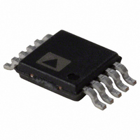
AD7942BRMZ Analog Devices Inc, AD7942BRMZ Datasheet

AD7942BRMZ
Specifications of AD7942BRMZ
Available stocks
Related parts for AD7942BRMZ
AD7942BRMZ Summary of contents
Page 1
FEATURES 14-bit resolution with no missing codes Throughput: 250 kSPS INL: ±0.4 LSB typical, ±1 LSB maximum (±0.0061% of FSR) SINAD kHz THD: −100 kHz Pseudo differential analog input range ...
Page 2
AD7942 TABLE OF CONTENTS Features .............................................................................................. 1 Applications ....................................................................................... 1 Application Diagram ........................................................................ 1 General Description ......................................................................... 1 Revision History ............................................................................... 2 Specifications ..................................................................................... 3 Timing Specifications .................................................................. 5 Absolute Maximum Ratings ............................................................ 7 ESD Caution .................................................................................. 7 Pin Configuration ...
Page 3
SPECIFICATIONS VDD = 2 5.5 V, VIO = 2 VDD, V Table 2. Parameter RESOLUTION ANALOG INPUT Voltage Range Absolute Input Voltage Analog Input CMRR Leakage Current Input Impedance ACCURACY No Missing Codes Differential Linearity Error ...
Page 4
AD7942 Parameter DIGITAL OUTPUTS Data Format Pipeline Delay POWER SUPPLIES VDD VIO VIO Range 4, 5 Standby Current Power Dissipation 6 TEMPERATURE RANGE Specified Performance 1 LSB means least significant bit. With input ...
Page 5
TIMING SPECIFICATIONS 1 VDD = 4 5 VIO = 2 5 VDD + 0.3 V, whichever is the lowest, unless otherwise stated, T Table 3. Parameter Conversion Time: CNV Rising Edge to ...
Page 6
AD7942 1 VDD = 2 4 VIO = 2 4 VDD + 0.3 V, whichever is the lowest, unless otherwise stated, T Table 4. Parameter Conversion Time: CNV Rising Edge to Data ...
Page 7
ABSOLUTE MAXIMUM RATINGS Table 5. Parameter Rating Analog Inputs IN IN− 1 GND − 0 VDD + 0 ±130 mA REF GND − 0 VDD + 0.3 V Supply Voltages VDD and ...
Page 8
AD7942 PIN CONFIGURATION AND FUNCTION DESCRIPTIONS Table 6. Pin Function Descriptions 1 Pin No. Mnemonic Type Description 1 REF AI Reference Input Voltage. The V as closely as possible μF capacitor. 2 VDD P Power Supply. 3 ...
Page 9
TYPICAL PERFORMANCE CHARACTERISTICS 1.00 POSITIVE INL = +0.22LSB NEGATIVE INL = –0.34LSB 0.75 0.50 0.25 0 –0.25 –0.50 –0.75 –1.00 0 4096 8192 CODE Figure 5. Integral Nonlinearity vs. Code 150,000 129,941 100,000 50,000 0 0 915 0 1FFD 1FFE ...
Page 10
AD7942 86 SNR 85 SINAD 84 ENOB 83 82 2.0 2.5 3.0 3.5 4.0 REFERENCE VOLTAGE (V) Figure 11. SNR, SINAD, and ENOB vs. Reference Voltage 5V, –10dB REF REF ...
Page 11
VDD + VIO 250 0 –55 –35 – TEMPERATURE (°C) Figure 17. Power-Down Currents vs. Temperature 1000 900 800 VDD = 5V 700 600 VDD = 2.5V 500 400 300 200 100 VIO ...
Page 12
AD7942 TERMINOLOGY Linearity Error or Integral Nonlinearity Error (INL) Linearity error refers to the deviation of each individual code from a line drawn from negative full scale through positive full scale. The point used as negative full scale occurs ½ ...
Page 13
THEORY OF OPERATION IN+ REF GND IN– CIRCUIT INFORMATION The AD7942 is a fast, low power, single-supply, precise 14-bit ADC using successive approximation architecture. The AD7942 is capable of converting 250,000 samples per second (250 kSPS) and powers down between ...
Page 14
AD7942 REF (NOTE 3) NOTE 1: SEE THE VOLTAGE REFERENCE INPUT SECTION FOR REFERENCE SELECTION. NOTE USUALLY A 10µF CERAMIC CAPACITOR (X5R). REF NOTE 3: SEE DRIVER AMPLIFIER CHOICE SECTION. NOTE 4: OPTIONAL FILTER. ...
Page 15
FREQUENCY (kHz) Figure 25. Analog Input CMRR vs. Frequency During the acquisition phase, the impedance of the analog input, IN+, can be modeled as a parallel combination of the Capacitor C and ...
Page 16
AD7942 Power Supply The AD7942 is specified over a wide operating range from 2 5 has, unlike other low voltage converters, a noise low enough to design a low supply (2.5 V) 14-bit resolu- tion system ...
Page 17
CS Mode 3-Wire Without Busy Indicator This mode is most often used when a single AD7942 is connected to an SPI-compatible digital host. The connection diagram is shown in Figure 30 and the corresponding timing diagram is shown in Figure ...
Page 18
AD7942 CS Mode 3-Wire with Busy Indicator This mode is most often used when a single AD7942 is connected to an SPI-compatible digital host with an interrupt input. The connection diagram is shown in Figure 32 and the corresponding timing ...
Page 19
CS Mode 4-Wire Without Busy Indicator This mode is most often used when multiple AD7942s are connected to an SPI-compatible digital host. A connection diagram using two AD7942s is shown in Figure 34 and the corresponding timing diagram is given ...
Page 20
AD7942 CS Mode 4-Wire with Busy Indicator This mode is most often used when a single AD7942 is connected to an SPI-compatible digital host with an interrupt input and to keep CNV (which is used to sample the analog input) ...
Page 21
Chain Mode Without Busy Indicator This mode can be used to daisy-chain multiple AD7942s on a 3-wire serial interface. This feature is useful for reducing component count and wiring connections, for example, in isolated multiconverter applications or for systems with ...
Page 22
AD7942 Chain Mode with Busy Indicator This mode can also be used to daisy-chain multiple AD7942s on a 3-wire serial interface while providing a busy indicator. This feature is useful for reducing component count and wiring connections, for example, in ...
Page 23
APPLICATION HINTS LAYOUT Design the PCB that houses the AD7942 so that the analog and digital sections are separated and confined to certain areas of the board. The pinout of the AD7942, with all its analog signals on the left ...
Page 24
... SEATING PLANE ORDERING GUIDE Model Temperature Range AD7942BRM –40°C to +85°C AD7942BRM-RL7 –40°C to +85°C 1 AD7942BRMZ –40°C to +85°C 1 AD7942BRMZ-RL7 –40°C to +85°C 1 AD7942BCPZRL –40°C to +85°C 1 AD7942BCPZRL7 –40°C to +85° EVAL-AD7942CBZ 1, 3 EVAL-CONTROL BRD3Z RoHS Compliant Part ...


