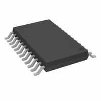
AD7730LBRU Analog Devices Inc, AD7730LBRU Datasheet - Page 41

AD7730LBRU
Manufacturer Part Number
AD7730LBRU
Description
IC ADC TRANSDUCER BRIDGE 24TSSOP
Manufacturer
Analog Devices Inc
Datasheet
1.AD7730LBRUZ.pdf
(52 pages)
Specifications of AD7730LBRU
Rohs Status
RoHS non-compliant
Number Of Bits
24
Sampling Rate (per Second)
600
Data Interface
DSP, Serial, SPI™
Number Of Converters
1
Power Dissipation (max)
125mW
Voltage Supply Source
Analog and Digital
Operating Temperature
-40°C ~ 85°C
Mounting Type
Surface Mount
Package / Case
24-TSSOP (0.173", 4.40mm Width)
For Use With
EVAL-AD7730LEBZ - BOARD EVALUATION FOR AD7730EVAL-AD7730EBZ - BOARD EVAL FOR AD7730
Available stocks
Company
Part Number
Manufacturer
Quantity
Price
Company:
Part Number:
AD7730LBRUZ
Manufacturer:
ADI
Quantity:
1 000
Company:
Part Number:
AD7730LBRUZ-REEL7
Manufacturer:
ADI
Quantity:
1 000
Long lead lengths from the bridge to the AD7730 facilitate the
pickup of mains frequency on the analog input, the reference
input and the power supply. The analog inputs to the AD7730
are buffered, which allows the user to connect whatever noise
reduction capacitors are necessary in the application. The AD7730
boasts excellent common-mode and normal- mode rejection of
mains frequency on both the analog and reference inputs. In
CHOP mode, care must be taken in choosing the output update
rate so it does not result in reducing line frequency rejection
(see DIGITAL FILTERING section). The input offset current
on the AD7730 is 10 nA maximum which results in a maxi-
mum, dc offset voltage of 1.75 mV in a 350
tion. Care should taken with inserting large source impedances
on the reference input pins as these inputs are not buffered and
the source impedances can result in gain errors.
In many load-cell applications, a portion of the dynamic range
of the bridge output is consumed by a pan weight or tare weight.
In such applications, the 6-bit TARE DAC of the AD7730 can
be used to adjust out this tare weight as outlined previously.
AC Excitation of Bridge
AC excitation of the bridge addresses many of the concerns with
thermocouple, offset and drift effects encountered in dc-excited
applications. In ac-excitation, the polarity of the excitation volt-
age to the bridge is reversed on alternate cycles. The result is the
elimination of dc errors at the expense of a more complex sys-
tem design. Figure 24 outlines the connections for an ac-excited
bridge application based on the AD7730.
The excitation voltage to the bridge must be switched on
alternate cycles. Transistors T1 to T4 in Figure 24 perform
the switching of the excitation voltage. These transistors can be
REV. A
T1
T3
OUT+
IN–
IN+
OUT–
T2
T4
Figure 24. Typical Connections for AC-Excited Bridge Application
EXCITATION VOLTAGE = +5V
AIN2(+)/D1
AIN2(–)/D0
REF IN(+)
REF IN(–)
AIN1(+)
AIN1(–)
bridge applica-
ACX
ACX
AV
DD
MUX
EXCITATION
CLOCK
AGND
AC
DV
–41–
BUFFER
DD
6-BIT
DAC
discrete matched bipolar or MOS transistors, or a dedicated
bridge driver chip such as the 4427 from Micrel can be used to
perform the task.
Since the analog input voltage and the reference voltage are
reversed on alternate cycles, the AD7730 must be synchronized
with this reversing of the excitation voltage. To allow the
AD7730 to synchronize itself with this switching, it provides the
logic control signals for the switching of the excitation voltage.
These signals are the nonoverlapping CMOS outputs ACX
and ACX.
One of the problems encountered with ac-excitation is the set-
tling time associated with the analog input signals after the
excitation voltage is switched. This is particularly true in appli-
cations where there are long lead lengths from the bridge to the
AD7730. It means that the converter could encounter errors
because it is processing signals which are not fully settled. The
AD7730 addresses this problem by allowing the user to program
a delay of up to 48.75 s between the switching of the ACX
signals and the processing of data at the analog inputs. This is
achieved using the DL bits of the Filter Register.
The AD7730 also scales the ACX switching frequency in accor-
dance with the output update rate. This avoids situations where
the bridge is switched at an unnecessarily faster rate than the
system requires.
The fact that the AD7730 can handle reference voltages which
are the same as the excitation voltages is particularly useful in
ac-excitation where resistor divider arrangements on the
reference input add to the settling time associated with the
switching.
+/–
+
DGND
PGA
AND CONTROL LOGIC
SERIAL INTERFACE
MICROCONTROLLER
POL
CALIBRATION
MODULATOR
SIGMA-DELTA A/D CONVERTER
SIGMA-
DELTA
RDY
REGISTER BANK
PROGRAMMABLE
AD7730
GENERATION
AD7730/AD7730L
DIGITAL
FILTER
CLOCK
RESET
MCLK OUT
MCLK IN
STANDBY
SYNC
SCLK
CS
DIN
DOUT


