AD673JNZ Analog Devices Inc, AD673JNZ Datasheet - Page 2
AD673JNZ
Manufacturer Part Number
AD673JNZ
Description
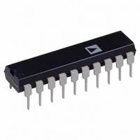
IC ADC 8BIT REF/CLK/COMP 20DIP
Manufacturer
Analog Devices Inc
Datasheet
1.AD673JNZ.pdf
(8 pages)
Specifications of AD673JNZ
Data Interface
Parallel
Number Of Bits
8
Sampling Rate (per Second)
33k
Number Of Converters
1
Voltage Supply Source
Dual ±
Operating Temperature
0°C ~ 70°C
Mounting Type
Through Hole
Package / Case
20-DIP (0.300", 7.62mm)
Resolution (bits)
8bit
Input Channel Type
Single Ended
Supply Current
15mA
Digital Ic Case Style
DIP
No. Of Pins
20
Operating Temperature Range
0°C To +70°C
Conversion Time
20µs
Rohs Compliant
Yes
Lead Free Status / RoHS Status
Lead free / RoHS Compliant
Available stocks
Company
Part Number
Manufacturer
Quantity
Price
Company:

Part Number:
AD673JNZ
Manufacturer:
AD
Quantity:
4 015


AD673–SPECIFICATIONS
Model
RESOLUTION
RELATIVE ACCURACY,
FULL-SCALE CALIBRATION
UNIPOLAR OFFSET
BIPOLAR OFFSET
DIFFERENTIAL NONLINEARITY,
TEMPERATURE RANGE
TEMPERATURE COEFFICIENTS
POWER SUPPLY REJECTION
ANALOG INPUT IMPEDANCE
ANALOG INPUT RANGES
OUTPUT CODING
LOGIC OUTPUT
LOGIC INPUTS
CONVERSION TIME, T
POWER SUPPLY
OPERATING CURRENT
NOTES
1
2
3
4
Specifications subject to change without notice.
Specifications shown in boldface are tested on all production units at final electrical test. Results from those tests are used to calculate outgoing quality levels. All min
and max specifications are guaranteed, although only those shown in boldface are tested on all production units.
Relative accuracy is defined as the deviation of the code transition points from the ideal transfer point on a straight line from the zero to the full scale of the device.
Full-scale calibration is guaranteed trimmable to zero with an external 200
Defined as the resolution for which no missing codes will occur.
The data output lines have active pull-ups to source 0 5 mA. The DATA READY line is open collector with a nominal 6 k
Full scale is defined as 10 volts minus 1 LSB, or 9.961 V.
T
T
Unipolar Offset
Bipolar Offset
Full-Scale Calibration
Positive Supply
Negative Supply
Unipolar
Bipolar
Unipolar
Bipolar
Output Sink Current
Output Source Current
Output Leakage
Input Current
Logic “1”
Logic “0”
T
V+
V–
V+
V–
A
A
MIN
+4.5
–15.75 V
–12.6 V
(V
(V
= T
= T
OUT
OUT
to T
MIN
MIN
= 0.4 V max, T
= 2.4 V min, T
MAX
V+
to T
to T
V–
V–
MAX
MAX
+5.5 V
–11.4 V
–14.25 V
2
A
4
l
MIN
and
MIN
to T
to T
2
MAX
MAX
3
)
)
(T
digital common, unless otherwise noted)
Min
8
8
0
3.0
0
–5
Positive True Binary
Positive True Offset Binary
3.2
0.5
2.0
10
+4.5
–11.4
A
= +25 C, V+ = +5 V, V– = –12 V or –15 V, all voltages measured with respect to
potentiometer in place of the 15
AD673J
Typ
8
5.0
20
+5.0
–15
15
9
–2–
2
Max
7.0
+10
+5
0.8
30
+7.0
–16.5
20
15
+70
1/2
1/2
1/2
1/2
1
1
2
2
2
2
40
100
Positive True Binary
Positive True Offset Binary
Min
8
8
–55
3.0
0
–5
3.2
0.5
2.0
10
+4.5
–11.4
fixed resistor.
internal pull-up resistor.
AD673S
Typ
8
5.0
20
+5.0
–15
15
9
2
Max
+125
7.0
+10
+5
0.8
30
+7.0
–16.5
20
15
1/2
1/2
1/2
1/2
1
1
2
2
2
2
40
100
REV. A
Units
Bits
LSB
LSB
LSB
LSB
LSB
Bits
Bits
LSB
LSB
LSB
LSB
LSB
LSB
k
V
V
mA
mA
V
V
V
V
mA
mA
C
A
A
s
Related parts for AD673JNZ
Image
Part Number
Description
Manufacturer
Datasheet
Request
R

Part Number:
Description:
±1.7g Dual-Axis IMEMS Accelerometer Evaluation Board
Manufacturer:
Analog Devices Inc
Datasheet:

Part Number:
Description:
Inertial Sensor Evaluation System
Manufacturer:
Analog Devices Inc
Datasheet:
Part Number:
Description:
Manufacturer:
Analog Devices Inc
Datasheet:
Part Number:
Description:
Manufacturer:
Analog Devices Inc
Datasheet:
Part Number:
Description:
Manufacturer:
Analog Devices Inc
Datasheet:
Part Number:
Description:
Manufacturer:
Analog Devices Inc
Datasheet:
Part Number:
Description:
Manufacturer:
Analog Devices Inc
Datasheet:
Part Number:
Description:
Manufacturer:
Analog Devices Inc
Datasheet:
Part Number:
Description:
Manufacturer:
Analog Devices Inc
Datasheet:
Part Number:
Description:
Manufacturer:
Analog Devices Inc
Datasheet:
Part Number:
Description:
Manufacturer:
Analog Devices Inc
Datasheet:
Part Number:
Description:
Manufacturer:
Analog Devices Inc
Datasheet:
Part Number:
Description:
Manufacturer:
Analog Devices Inc
Datasheet: