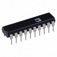
AD673JNZ Analog Devices Inc, AD673JNZ Datasheet - Page 7

AD673JNZ
Manufacturer Part Number
AD673JNZ
Description
IC ADC 8BIT REF/CLK/COMP 20DIP
Manufacturer
Analog Devices Inc
Datasheet
1.AD673JNZ.pdf
(8 pages)
Specifications of AD673JNZ
Data Interface
Parallel
Number Of Bits
8
Sampling Rate (per Second)
33k
Number Of Converters
1
Voltage Supply Source
Dual ±
Operating Temperature
0°C ~ 70°C
Mounting Type
Through Hole
Package / Case
20-DIP (0.300", 7.62mm)
Resolution (bits)
8bit
Input Channel Type
Single Ended
Supply Current
15mA
Digital Ic Case Style
DIP
No. Of Pins
20
Operating Temperature Range
0°C To +70°C
Conversion Time
20µs
Rohs Compliant
Yes
Lead Free Status / RoHS Status
Lead free / RoHS Compliant
Available stocks
Company
Part Number
Manufacturer
Quantity
Price
Company:
Part Number:
AD673JNZ
Manufacturer:
AD
Quantity:
4 015
In systems where this read-write interface is used, at least
30 microseconds (the maximum conversion time) must be al-
lowed to pass between starting a conversion and reading the re-
sults. This delay or “time-out” period can be implemented in a
short software routine such as a countdown loop, enough
dummy instructions to consume 30 microseconds, or enough
actual useful instructions to consume the required time. In tightly-
timed systems, the DR line may be read through an external
three-state buffer to determine precisely when a conversion is
complete. Higher-speed systems may choose to use DR to signal
an interrupt to the processor at the end of a conversion.
REV. A
Figure 12. Typical AD673 Timing Diagram
–7–
CONVERT Pulse Generation
The AD673 is tested with a CONVERT pulse width of 500 ns
and will typically operate with a pulse as short as 300 ns. How-
ever, some microprocessors produce active WR pulses which are
shorter than this. Either of the circuits shown in Figure 13 can
be used to generate an adequate CONVERT pulse for the
AD673. In both circuits, the short low-going WR pulse sets the
CONVERT line high through a flip-flop. The rising edge of DR
(which signifies that the internal logic has been reset) resets
the flip-flop and brings CONVERT low, which starts the
conversion.
Note that t
conversion contains a Logic 1 on the LSB. This means that the
actual CONVERT pulse generated by the circuits in Figure 13
will vary slightly in width.
Figure 13a. Using 74LS00
DSC
is slightly longer when the result of the previous
Figure 13b. Using 1/2 74LS74
AD673


