6450128-2 TE Connectivity, 6450128-2 Datasheet - Page 4
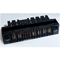
6450128-2
Manufacturer Part Number
6450128-2
Description
MBXL R/A HDR STR 2P+24S+2P
Manufacturer
TE Connectivity
Specifications of 6450128-2
Product Series
XL
Connector Type
Header
Mount Angle
Right Angle
Termination Style
Solder
Mating Type
Squeeze-to-Release
Pcb Mount Retention
With
Guides
With
Voltage Rating (signal) (vac)
60
Voltage Rating (power) (vdc)
200
Termination Post Length (mm [in])
3.43 [0.135]
Sequencing
No
Pcb Mount Retention Type
Retention Clip/Post
Connector Configuration Orientation
Left-to-Right
Centerline, Dc Module (mm [in])
6.35 [0.250]
Centerline, Matrix (mm [in])
2.54 x 2.54 [.100 x .100]
Contact Type
Pin
Contact Material (power)
High Conductivity Copper
Contact Material (signal)
Copper Alloy
Contact Plating, Mating Area, Material
Gold (30)
Connector Style
Plug
Housing Material
High Temperature Thermoplastic
Total Number Of Dc Power
4
Total Number Of Signal
24
Connector Contact Configuration (no. Of Pos./type)
2/DC Power, 24/Signal, 2/DC Power
Rohs/elv Compliance
RoHS compliant, ELV compliant
Lead Free Solder Processes
Wave solder capable to 240°C, Wave solder capable to 260°C, Wave solder capable to 265°C
Rohs/elv Compliance History
Always was RoHS compliant
Application Use
Cable-to-Board


Rev C
Mechanical shock.
Durability.
Mating force.
Unmating force.
Compliant pin insertion.
Radial hole distortion.
Compliant pin retention.
Component heat resistance to
wave soldering.
Solderability dip test.
Thermal shock.
Test Description
No discontinuities of 1 microsecond
or longer duration.
See Note.
See Note.
9 N [2 lbf] maximum for power
contact.
Average mating force for signal
contacts shall be less than 1.7 N [6
ozf] per contact.
2.2 N [8 ozf] minimum per power
contact.
0.2 N [.7 ozf] minimum per signal
contact.
111.2 N [25 lbf] maximum per pin.
0.070 mm [.00276 in] maximum
radial distortion.
0.008 mm [.00032 in] minimum
copper hole wall remaining.
6.7 N [1.5 lbf] minimum per pin.
See Note.
Solderable area shall have a
minimum of 95% solder coverage.
See Note.
See Note.
Figure 3 (continued)
ENVIRONMENTAL
Requirement
EIA-364-27, Method A.
Subject mated specimens to 50 G's
half-sine shock pulses of 11
milliseconds duration. Three
shocks in each direction applied
along 3 mutually perpendicular
planes, 18 total shocks.
EIA-364-9.
Mate and unmate specimens for
250 cycles at a maximum rate of
500 cycles per hour.
EIA-364-13.
Measure force necessary to mate
specimens at a maximum rate of
12.7 mm [.5 in] per minute.
EIA-364-13.
Measure force necessary to
unmate specimens at a maximum
rate of 12.7 mm [.5 in] per minute.
TE Spec. 109-41.
Measure force necessary to
correctly apply a specimen to a
printed circuit board at a maximum
rate of 12.7 mm [.5 in] per minute.
TE Spec. 109-136.
Measure at 0.2 to 0.5 mm [.008 to
.020 in] depth.
TE Spec 109-30-1.
Measure force necessary to
remove a correctly applied
specimen from its printed circuit
board at a maximum rate of 12.7
mm [.5 in] per minute.
TE Spec. 109-202, Condition B.
TE Spec. 109-11-11, Test Method
A.
EIA-364-32.
Subject mated specimens to 36
cycles between -20 and 105° C.
Procedure
108-1973
4 of 7
Related parts for 6450128-2
Image
Part Number
Description
Manufacturer
Datasheet
Request
R

Part Number:
Description:
SB 04P 3.50mm Grn/Gry/Blue/Wht
Manufacturer:
BLOCKMASTER ELECTRONICS
Part Number:
Description:
SB 04P 3.50mm Gry/Grn/Wht/Blue
Manufacturer:
BLOCKMASTER ELECTRONICS

Part Number:
Description:
High Speed / Modular Connectors 30P HEADER ASSY
Manufacturer:
TE Connectivity
Datasheet:

Part Number:
Description:
High Speed / Modular Connectors REC 6X005P R/A LT B-PLANE HS3
Manufacturer:
TE Connectivity
Datasheet:

Part Number:
Description:
High Speed / Modular Connectors 2MM HM RCPT 50P R/A AU
Manufacturer:
TE Connectivity
Datasheet:

Part Number:
Description:
High Speed / Modular Connectors 2MM HM RCPT 50P R/A AU
Manufacturer:
TE Connectivity
Datasheet:


Part Number:
Description:
Manufacturer:
TE Connectivity
Datasheet:


Part Number:
Description:
Manufacturer:
TE Connectivity
Datasheet:

Part Number:
Description:
Manufacturer:
TE Connectivity
Datasheet:

Part Number:
Description:
Manufacturer:
TE Connectivity
Datasheet: