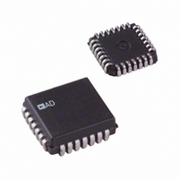
AD7828KP Analog Devices Inc, AD7828KP Datasheet - Page 6

AD7828KP
Manufacturer Part Number
AD7828KP
Description
IC ADC 8BIT LC2MOS 8CH 28-PLCC
Manufacturer
Analog Devices Inc
Datasheet
1.AD7828LRS-REEL.pdf
(16 pages)
Specifications of AD7828KP
Data Interface
Parallel
Rohs Status
RoHS non-compliant
Number Of Bits
8
Sampling Rate (per Second)
50k
Number Of Converters
3
Power Dissipation (max)
100mW
Voltage Supply Source
Single Supply
Operating Temperature
0°C ~ 70°C
Mounting Type
Surface Mount
Package / Case
28-LCC (J-Lead)
Resolution (bits)
8bit
Sampling Rate
50kSPS
Input Channel Type
Differential
Supply Voltage Range - Analog
4.75V To 5.25V
Supply Current
16mA
Digital Ic Case Style
LCC
Lead Free Status / RoHS Status
Contains lead / RoHS non-compliant
Available stocks
Company
Part Number
Manufacturer
Quantity
Price
Company:
Part Number:
AD7828KP
Manufacturer:
AD
Quantity:
1 010
Part Number:
AD7828KP
Manufacturer:
ADI/亚德诺
Quantity:
20 000
Company:
Part Number:
AD7828KP-REEL
Manufacturer:
Analog Devices Inc
Quantity:
10 000
Company:
Part Number:
AD7828KPZ
Manufacturer:
Analog Devices Inc
Quantity:
10 000
Part Number:
AD7828KPZ
Manufacturer:
ADI/亚德诺
Quantity:
20 000
AD7824/AD7828
OPERATIONAL DIAGRAM
The AD7824 is a 4-channel 8-bit ADC and the AD7828 is an
8-channel 8-bit ADC. Operational diagrams for both of these
devices are shown in Figures 3 and 4. The addition of just a 5 V
reference allows the devices to perform the analog-to-digital function.
CIRCUIT INFORMATION
BASIC DESCRIPTION
The AD7824/AD7828 uses a half-flash conversion technique
whereby two 4-bit flash ADCs are used to achieve an 8-bit result.
Each 4-bit flash ADC contains 15 comparators that compare
the unknown input to a reference ladder to get a 4-bit result.
For a full 8-bit reading to be realized, the upper 4-bit flash, the
most significant (MS) flash, performs a conversion to provide
the four most significant data bits. An internal DAC, driven by
the four MSBs, then recreates an analog approximation of the
input voltage. This analog result is subtracted from the input,
and the difference is converted by the lower flash ADC, the least
significant (LS) flash, to provide the four least significant bits of
the output data. The most significant flash ADC also has one
additional comparator to detect overrange on the analog input.
ANALOG INPUTS
ANALOG INPUTS
P CONTROL INPUT
P CONTROL INPUT
STATUS OUTPUT
STATUS OUTPUT
DATA BUS
DATA BUS
0V TO 5V
0V TO 5V
Figure 3. AD7824 Operational Diagram
Figure 4. AD7828 Operational Diagram
P 4LSB
P 4LSB
12
10
11
12
13
14
10
11
1
2
3
4
5
6
7
8
9
1
2
3
4
5
6
7
8
9
NC = NO CONNECT
NC = NO CONNECT
NC
DB0
DB1
DB2
DB3
RD
INT
GND
AIN4
AIN3
AIN2
AIN1
NC
DB0
DB1
DB2
DB3
RD
INT
GND
AIN6
AIN5
AIN4
AIN3
AIN2
AIN1
AD7828
AD7824
V
V
V
V
REF
REF
REF
REF
AIN7
AIN8
RDY
DB5
DB4
RDY
DB7
DB6
DB5
DB4
DB7
DB6
V
V
NC
A0
A2
CS
CS
DD
A1
(+)
(–)
DD
A0
(+)
(–)
A1
28
27
26
25
24
23
22
21
20
19
18
17
16
15
24
23
22
21
20
19
18
17
16
15
14
13
5V
STATUS OUTPUT
5V
STATUS OUTPUT
5V
5V
P CONTROL INPUT
P CONTROL INPUT
ANALOG INPUTS
0V TO 5V
BUS
DATA BUS
BUS
DATA BUS
P ADDRESS
P 4MSB
P ADDRESS
P 4MSB
–6–
APPLYING THE AD7824/AD7828
REFERENCE AND INPUT
The two reference inputs on the AD7824/AD7828 are fully differ-
ential and define the zero to full-scale input range of the ADC.
As a result, the span of the analog input voltage for all channels
can easily be varied. By reducing the reference span, V
V
increased (e.g., if V
reference arrangement also facilitates ratiometric operation.
This reference flexibility also allows the input channel voltage
span to be offset from zero. The voltage at V
input level for all channels, which produces a digital output of
all zeroes. Therefore, although the analog inputs are not them-
selves differential, they have nearly differential input capability
in most measurement applications because of the reference
design. Figures 5 to 7 show some of the configurations that are
possible.
Figure 6. External Reference Using the AD580, Full-Scale
Input is 2.5 V
REF
5V
(–), to less than 5 V, the sensitivity of the converter can be
5V
0.1 F
Figure 7. Input Not Referenced to GND
Figure 5. Power Supply as Reference
5V
V
V
V
V
0.1 F
IN
IN
IN
IN
DATA =
*
*
*
(+)
(–)
ADDITIONAL PINS OMITTED FOR CLARITY.
ONLY CHANNEL 1 SHOWN.
(+)
(–)
ADDITIONAL PINS OMITTED FOR CLARITY.
ONLY CHANNEL 1 SHOWN.
ADDITIONAL PINS OMITTED FOR CLARITY.
ONLY CHANNEL 1 SHOWN.
47 F
REF
0.1 F
V1 – V2
= 2 V then 1 LSB = 7.8 mV). The input/
V
47 F
IN
AD580
(+)
V
IN
47 F
(+)
V1
V2
256 (FOR ALL CHANNELS)
10 F
AIN1
GND
V
V
V
AIN1
GND
V
V
V
DD
REF
REF
DD
REF
REF
(+)
(–)
(+)
(–)
AD7824*
AD7828*
AD7824*
AD7828*
0.1 F
REF
AIN1
GND
V
V
V
DB7
DB0
DD
REF
REF
(–) sets the
(+)
(–)
DATA
AD7824*
AD7828*
REF
REV. F
(+) to


