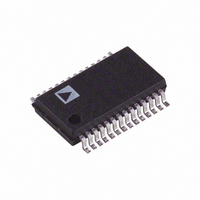
AD9225ARS Analog Devices Inc, AD9225ARS Datasheet - Page 3

AD9225ARS
Manufacturer Part Number
AD9225ARS
Description
IC ADC 12BIT 25MSPS 28-SSOP
Manufacturer
Analog Devices Inc
Datasheet
1.AD9225ARZ.pdf
(25 pages)
Specifications of AD9225ARS
Mounting Type
Surface Mount
Package / Case
28-SSOP (0.200", 5.30mm Width)
Rohs Status
RoHS non-compliant
Number Of Bits
12
Sampling Rate (per Second)
25M
Data Interface
Parallel
Number Of Converters
7
Power Dissipation (max)
373mW
Voltage Supply Source
Single Supply
Operating Temperature
-40°C ~ 85°C
Peak Reflow Compatible (260 C)
No
No. Of Bits
12 Bit
Leaded Process Compatible
No
No. Of Channels
2
Interface Type
Parallel
For Use With
AD9225-EB - BOARD EVAL FOR AD9225
Lead Free Status / RoHS Status
Contains lead / RoHS non-compliant
Available stocks
Company
Part Number
Manufacturer
Quantity
Price
Company:
Part Number:
AD9225ARS
Manufacturer:
ADI
Quantity:
288
Part Number:
AD9225ARS
Manufacturer:
ADI/亚德诺
Quantity:
20 000
Part Number:
AD9225ARSRL
Manufacturer:
ADI/亚德诺
Quantity:
20 000
Company:
Part Number:
AD9225ARSZ
Manufacturer:
ADI
Quantity:
1 000
Part Number:
AD9225ARSZ
Manufacturer:
ADI/亚德诺
Quantity:
20 000
Company:
Part Number:
AD9225ARSZRL
Manufacturer:
ADI
Quantity:
1 000
Rev. C
AC SPECIFICATIONS
Parameter
SIGNAL-TO-NOISE AND DISTORTION RATIO (S/N+D)
SIGNAL-TO-NOISE RATIO (SNR)
TOTAL HARMONIC DISTORTION (THD)
SPURIOUS FREE DYNAMIC RANGE
Specifications subject to change without notice.
DIGITAL SPECIFICATIONS
Parameter
LOGIC INPUTS
LOGIC OUTPUTS
LOGIC OUTPUTS (with DRVDD = 3 V)
Specifications subject to change without notice.
SWITCHING SPECIFICATIONS
Parameter
Clock Period*
CLOCK Pulse Width High
CLOCK Pulse Width Low
Output Delay
Pipeline Delay (Latency)
*The clock period may be extended to 1 ms without degradation in specified performance @ 25 ∞C.
Specifications subject to change without notice.
f
f
f
f
f
f
f
f
Full Power Bandwidth
Small Signal Bandwidth
Aperture Delay
Aperture Jitter
Acquisition to Full-Scale Step
High Level Input Voltage
Low Level Input Voltage
High Level Input Current (V
Low Level Input Current (V
Input Capacitance
High Level Output Voltage (I
High Level Output Voltage (I
Low Level Output Voltage (I
Low Level Output Voltage (I
Output Capacitance
High Level Output Voltage (I
High Level Output Voltage (I
Low Level Output Voltage (I
Low Level Output Voltage (I
INPUT
INPUT
INPUT
INPUT
INPUT
INPUT
INPUT
INPUT
= 2.5 MHz
= 10 MHz
= 2.5 MHz
= 10 MHz
= 2.5 MHz
= 10 MHz
= 2.5 MHz
= 10 MHz
IN
IN
OL
OL
OL
OL
OH
OH
OH
OH
= 0 V)
(AVDD = 5 V, DRVDD = 5 V, f
otherwise noted.)
= DRVDD)
= 1.6 mA)
= 50 mA)
= 1.6 mA)
= 50 mA)
= 50 mA)
= 0.5 mA)
= 50 mA)
= 0.5 mA)
(AVDD = 5 V, DRVDD = 5 V, unless otherwise noted.)
(T
MIN
to T
Min
69.0
68.2
73
67.4
66.7
72.5
Symbol
V
V
I
I
C
V
V
V
V
C
V
V
V
V
Symbol
t
t
t
t
MAX
C
CH
CL
OD
IH
IL
IH
IL
OH
OH
OL
OL
OH
OH
OL
OL
IN
OUT
with AVDD = 5 V, DRVDD = 5 V, C
SAMPLE
–3–
= 25 MSPS, VREF = 2.0 V, T
Typ
70.7
69.6
71
70
–82
–81
–85
–83
105
105
1
1
10
Min
3.5
–10
–10
4.5
2.4
2.95
2.80
Min
40
18
18
13
Max
–72
–71.5
Typ
5
5
Typ
3
L
= 20 pF)
MIN
to T
MAX
, Differential Input unless
dB
dB
dB
dB
Unit
dB
dB
dB
dB
MHz
MHz
ns
ps rms
ns
Max
1.0
+10
+10
0.4
0.1
0.4
0.05
Max
Unit
V
V
mA
mA
pF
V
V
V
V
V
V
V
V
Unit
ns
ns
ns
ns
Clock Cycles
pF
AD9225


