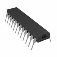
AD7880BNZ Analog Devices Inc, AD7880BNZ Datasheet - Page 3

AD7880BNZ
Manufacturer Part Number
AD7880BNZ
Description
IC ADC 12BIT MONO LOW PWR 24DIP
Manufacturer
Analog Devices Inc
Datasheet
1.AD7880BRZ-REEL.pdf
(16 pages)
Specifications of AD7880BNZ
Data Interface
Parallel
Operating Temperature
-40°C ~ 85°C
Number Of Bits
12
Sampling Rate (per Second)
66k
Number Of Converters
1
Power Dissipation (max)
50mW
Voltage Supply Source
Single Supply
Mounting Type
Through Hole
Package / Case
24-DIP (0.300", 7.62mm)
Resolution (bits)
12bit
Input Channel Type
Single Ended
Supply Voltage Range - Analogue
4.75V To 5.25V
Supply Current
10mA
No. Of Pins
24
Sampling Rate
66kSPS
Rohs Compliant
Yes
Lead Free Status / RoHS Status
Lead free / RoHS Compliant
Available stocks
Company
Part Number
Manufacturer
Quantity
Price
REV. 0
TIMING CHARACTERISTICS
Parameter
t
t
t
t
t
t
t
t
NOTES
1
2
3
CAUTION
ESD (electrostatic discharge) sensitive device. Electrostatic charges as high as 4000 V readily
accumulate on the human body and test equipment and can discharge without detection.
Although the AD7880 features proprietary ESD protection circuitry, permanent damage may
occur on devices subjected to high energy electrostatic discharges. Therefore, proper ESD
precautions are recommended to avoid performance degradation or loss of functionality.
Timing specifications in bold print are 100% production tested. All other times are sample tested at +25 C to ensure compliance. All input signals are specified with
t
t
1
2
3
4
5
6
7
8
tr = tf = 5 ns (10% to 90% of 5 V) and timed from a voltage level of 1.6 V.
lated back to remove the effects of charging the 50 pF capacitor. This means that the time, t
the part and as such is independent of external bus loading capacitances.
DB0 – DB11
7
8
2
3
is measured with the load circuit of Figure 2 and defined as the time required for an output to cross 0.8 V or 2.4 V.
is derived from the measured time taken by the data outputs to change by 0.5 V when loaded with the circuit of Figure 2. The measured number is then extrapo-
CONVST
Figure 2. Load Circuit for Access and Relinquish Time
BUSY
RD
CS
TO OUTPUT
t
1
Figure 1. Timing Diagram
PIN
t
Limit at +25 C
(All Versions)
50
130
0
0
0
60
57
5
50
2
50pF
THREE-STATE
TRACK/HOLD
GOES INTO HOLD
t
CONVERT
1.6mA
200µA
1
(V
t
3
DD
Limit at T
(All Versions)
50
130
0
0
0
75
70
5
50
= +5 V
t
4
+
t
7
2.1V
t
6
VALID
DATA
5%, V
t
t
MIN
5
8
, T
REF
MAX
= V
–3–
DD
CS
1
1
0
0
ABSOLUTE MAXIMUM RATINGS*
V
V
AGND to DGND . . . . . . . . . . . . . . . . . –0.3 V to V
V
V
V
V
Digital Inputs to DGND . . . . . . . . . . . –0.3 V to V
Digital Outputs to DGND . . . . . . . . . . –0.3 V to V
Operating Temperature Range
Lead Temperature (Soldering, 10 secs) . . . . . . . . . . . . +300 C
Power Dissipation (Any Package) to +75 C . . . . . . . . 450 mW
Derates above +75 C by . . . . . . . . . . . . . . . . . . . . . 10 mW/ C
*Stresses above those listed under “Absolute Maximum Ratings” may cause
, AGND = DGND = 0 V)
permanent damage to the device. This is a stress rating only and functional
operation of the device at these or any other conditions above those listed in the
operational sections of this specification is not implied. Exposure to absolute
maximum rating conditions for extended periods may affect device reliability.
DD
DD
INA
INA
INA
REF
Industrial (B, C Versions) . . . . . . . . . . . . . –40 C to +85 C
Storage Temperature Range . . . . . . . . . . . –65 C to +150 C
, V
to AGND . . . . . . . . . . . . . . . . . . . . . . . . . –0.3 V to +7 V
to DGND . . . . . . . . . . . . . . . . . . . . . . . . . –0.3 V to +7 V
to AGND (Figure 6) . . . . . . . . . –0.6 V to 2 V
to AGND (Figure 7) . . . . . –V
8
to AGND . . . . . . . . . . . . . . . . . . . . . . . . . . 0.3 V to V
, quoted in the timing characteristics is the true bus relinquish time of
INB
Units
ns min
ns min
ns min
ns min
ns min
ns min
ns max
ns min
ns max
to AGND (Figure 5) . . . . . . –0.3 V to V
CONVST
1
j
1
1
Table I. Truth Table
Conditions/Comments
CONVST Pulse Width
CONVST to BUSY Falling Edge
BUSY to CS Setup Time
CS to RD Setup Time
CS to RD Hold Time
RD Pulse Width
Data Access Time after RD
Bus Relinquish Time after RD
RD
X
1
0
1
WARNING!
DD
Function
Not Selected
Start Conversion g
Enable ADC Data
Data Bus Three Stated
– 0.3 V to V
ESD SENSITIVE DEVICE
AD7880
DD
DD
DD
DD
DD
DD
+ 0.3 V
+ 0.3 V
+ 0.6 V
+ 0.3 V
+ 0.3 V
+ 0.3 V
DD


