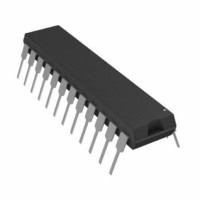
AD7880BNZ Analog Devices Inc, AD7880BNZ Datasheet - Page 4

AD7880BNZ
Manufacturer Part Number
AD7880BNZ
Description
IC ADC 12BIT MONO LOW PWR 24DIP
Manufacturer
Analog Devices Inc
Datasheet
1.AD7880BRZ-REEL.pdf
(16 pages)
Specifications of AD7880BNZ
Data Interface
Parallel
Operating Temperature
-40°C ~ 85°C
Number Of Bits
12
Sampling Rate (per Second)
66k
Number Of Converters
1
Power Dissipation (max)
50mW
Voltage Supply Source
Single Supply
Mounting Type
Through Hole
Package / Case
24-DIP (0.300", 7.62mm)
Resolution (bits)
12bit
Input Channel Type
Single Ended
Supply Voltage Range - Analogue
4.75V To 5.25V
Supply Current
10mA
No. Of Pins
24
Sampling Rate
66kSPS
Rohs Compliant
Yes
Lead Free Status / RoHS Status
Lead free / RoHS Compliant
Available stocks
Company
Part Number
Manufacturer
Quantity
Price
AD7880
Model
AD7880BN –40 C to +85 C
AD7880BQ –40 C to +85 C
AD7880CN –40 C to +85 C
AD7880CQ –40 C to +85 C
AD7880BR
AD7880CR –40 C to +85 C
*N = Plastic DIP; Q = Cerdip; R = SOIC (Small Outline Integrated Circuit).
Pin
No.
10
11 . . . 22
23
24
1
2
3
4
5
6
7
8
9
Temperature
Range
–40 C to +85 C
Pin
Mnemonic Function
V
V
AGND
V
CS
CONVST
RD
BUSY
CLKIN
DGND
DB0–DB11 Three-State Data Outputs. These become active when CS and RD are brought low.
MODE
V
INA
INB
REF
DD
ORDERING GUIDE
Analog Input.
Analog Input.
Analog Ground.
Voltage Reference Input. This is normally tied to V
Chip Select. Active Low Logic input. The device is selected when this input is active.
Convert Start. A low to high transition on this input puts the track/hold into hold mode and starts con-
version. This input is asynchronous to the CLKIN and is independent of CS and RD.
Read. Active Low Logic Input. This input is used in conjunction with CS low to enable data outputs.
Active Low Logic Output. This status line indicates converter status. BUSY is low during conversion.
Clock Input. TTL-compatible logic input. Used as the clock source for the A/D converter. The mark/
space ratio of the clock can vary from 40/60 to 60/40.
Digital Ground.
MODE Input. This input is used to put the device into the power save mode (MODE = 0 V). During
normal operation, the MODE input will be a logic high (MODE = V
Power Supply. This is nominally +5 V.
Full-Scale
Error
(LSBs)
15
15
15
5
5
5
Bipolar
Zero
Error
(LSBs)
10
10
5
5
10
5
PIN FUNCTION DESCRIPTION
Package
Option*
N-24
Q-24
N-24
Q-24
R-24
R-24
–4–
DD
.
CONVST
AGND
CLKIN
DGND
BUSY
V
V
V
DB0
DB1
REF
PIN CONFIGURATION
INA
INB
RD
CS
10
11
12
1
2
3
4
5
6
7
8
9
(Not to Scale)
DD
AD7880
TOP VIEW
).
24
23
22
21
20
19
18
17
16
15
14
13
DB6
DB5
DB4
MODE
DB10
DB9
DB7
DB3
DB2
V
DB11
DB8
DD
REV. 0


