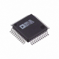
AD9240AS Analog Devices Inc, AD9240AS Datasheet - Page 8

AD9240AS
Manufacturer Part Number
AD9240AS
Description
IC ADC 14BIT 10MSPS 44-MQFP
Manufacturer
Analog Devices Inc
Datasheet
1.AD9240ASZ.pdf
(24 pages)
Specifications of AD9240AS
Mounting Type
Surface Mount
Rohs Status
RoHS non-compliant
Number Of Bits
14
Sampling Rate (per Second)
10M
Data Interface
Parallel
Number Of Converters
7
Power Dissipation (max)
330mW
Voltage Supply Source
Analog and Digital
Operating Temperature
-40°C ~ 85°C
Package / Case
44-MQFP, 44-PQFP
Power Dissipation Pd
330mW
Input Channels Per Adc
2
No. Of Channels
2
Peak Reflow Compatible (260 C)
No
Sample Rate
10MSPS
Supply Voltage Max
5V
No. Of Bits
14 Bit
For Use With
AD9240-EB - BOARD EVAL FOR AD9240
Lead Free Status / RoHS Status
Contains lead / RoHS non-compliant
Available stocks
Company
Part Number
Manufacturer
Quantity
Price
Company:
Part Number:
AD9240AS
Manufacturer:
AD
Quantity:
5 510
Part Number:
AD9240AS
Manufacturer:
ADI/亚德诺
Quantity:
20 000
Company:
Part Number:
AD9240ASRL
Manufacturer:
Analog Devices Inc
Quantity:
10 000
Company:
Part Number:
AD9240ASZ
Manufacturer:
ADI
Quantity:
850
Company:
Part Number:
AD9240ASZ
Manufacturer:
Analog Devices Inc
Quantity:
10 000
Part Number:
AD9240ASZ
Manufacturer:
ADI/亚德诺
Quantity:
20 000
Company:
Part Number:
AD9240ASZRL
Manufacturer:
MAXIM
Quantity:
495
AD9240
INTRODUCTION
The AD9240 uses a four-stage pipeline architecture with a
wideband input sample-and-hold amplifier (SHA) implemented
on a cost-effective CMOS process. Each stage of the pipeline,
excluding the last, consists of a low resolution flash A/D con-
nected to a switched capacitor DAC and interstage residue
amplifier (MDAC). The residue amplifier amplifies the differ-
ence between the reconstructed DAC output and the flash input
for the next stage in the pipeline. One bit of redundancy is used
in each of the stages to facilitate digital correction of flash er-
rors. The last stage simply consists of a flash A/D.
The pipeline architecture allows a greater throughput rate at the
expense of pipeline delay or latency. This means that while the
converter is capable of capturing a new input sample every clock
cycle, it actually takes three clock cycles for the conversion to be
fully processed and appear at the output. This latency is not a
concern in most applications. The digital output, together with
the out-of-range indicator (OTR), is latched into an output
buffer to drive the output pins. The output drivers can be con-
figured to interface with +5 V or +3.3 V logic families.
The AD9240 uses both edges of the clock in its internal timing
circuitry (see Figure 1 and specification page for exact timing
requirements). The A/D samples the analog input on the rising
edge of the clock input. During the clock low time (between the
falling edge and rising edge of the clock), the input SHA is in
the sample mode; during the clock high time it is in the hold
mode. System disturbances just prior to the rising edge of the
clock and/or excessive clock jitter may cause the input SHA to
acquire the wrong value, and should be minimized.
Speed/Power Programmability
The AD9240’s maximum conversion rate and associated power
dissipation can be set using the part’s BIAS pin. A simplified
diagram of the on-chip circuitry associated with the BIAS pin is
shown in Figure 20.
The value of R
maximum sample rate and power dissipation of the AD9240. A
typical plot of S/(N+D) @ f
R
at varying R
typical performance vs. R
specifications in this data sheet reflect performance at a fixed
R
BIAS
BIAS
is shown in Figure 21. A similar plot of power vs. f
= 2 k .
BIAS
BIAS
is shown in Figure 22. These plots indicate
AD9240
can be varied over a limited range to set the
BIAS
Figure 20.
IN
. Note that all other plots and
= Nyquist vs. f
ADC
I
FIXED
BIAS
BIAS
CLK
R
BIAS
at varying
CLK
–8–
Figure 22. Power Dissipation vs. Clock Frequency for
Varying R
ANALOG INPUT AND REFERENCE OVERVIEW
Figure 23, a simplified model of the AD9240, highlights the rela-
tionship between the analog inputs, VINA, VINB, and the ref-
erence voltage, VREF. Like the voltage applied to the top of
the resistor ladder in a flash A/D converter, the value VREF defines
the maximum input voltage to the A/D core. The minimum input
voltage to the A/D core is automatically defined to be –VREF.
Figure 21. SINAD vs. Clock Frequency for Varying R
Values (V
Figure 23. Equivalent Functional Input Circuit
400
350
300
250
200
150
100
70
60
50
40
30
10
80
20
0
BIAS
2
CM
1
= 2.5 V, A
Values
VINA
VINB
4
6
CLOCK FREQUENCY – MHz
CLOCK FREQUENCY – MHz
IN
V
8
AD9240
CORE
= –0.5 dB, 5 V Span, f
R
10
R
BIAS
BIAS
R
BIAS
= 10k
12
= 20k
CORE
+VREF
–VREF
= 200k
A/D
14
10
16
14
R
R
18
IN
BIAS
BIAS
4k
2k
= f
=
=
20
20
CLK
REV.
BIAS
/2)
B


