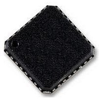
AD9649BCPZ-65 Analog Devices Inc, AD9649BCPZ-65 Datasheet - Page 19

AD9649BCPZ-65
Manufacturer Part Number
AD9649BCPZ-65
Description
IC ADC 14BIT 65MSPS 32LFCSP
Manufacturer
Analog Devices Inc
Datasheet
1.AD9649BCPZRL7-20.pdf
(32 pages)
Specifications of AD9649BCPZ-65
Data Interface
Serial, SPI™
Number Of Bits
14
Sampling Rate (per Second)
65M
Number Of Converters
1
Power Dissipation (max)
87.5mW
Voltage Supply Source
Analog and Digital
Operating Temperature
-40°C ~ 85°C
Mounting Type
Surface Mount
Package / Case
32-VFQFN, CSP Exposed Pad
Resolution (bits)
14bit
Sampling Rate
65MSPS
Input Channel Type
Differential
Supply Voltage Range - Analog
1.7V To 1.9V
Supply Voltage Range - Digital
1.7V To 3.6V
Lead Free Status / RoHS Status
Lead free / RoHS Compliant
Available stocks
Company
Part Number
Manufacturer
Quantity
Price
Company:
Part Number:
AD9649BCPZ-65
Manufacturer:
AD
Quantity:
3 200
VOLTAGE REFERENCE
A stable and accurate 1.0 V voltage reference is built into the
AD9649. The VREF can be configured using either the internal
1.0 V reference or an externally applied 1.0 V reference voltage.
The various reference modes are summarized in the sections
that follow. The Reference Decoupling section describes the
best practices PCB layout of the reference.
Internal Reference Connection
A comparator within the AD9649 detects the potential at the
SENSE pin and configures the reference into two possible modes,
which are summarized in Table 10. If SENSE is grounded, the
reference amplifier switch is connected to the internal resistor
divider (see Figure 43), setting VREF to 1.0 V.
If the internal reference of the AD9649 is used to drive multiple
converters to improve gain matching, the loading of the reference
by the other converters must be considered. Figure 44 shows
how the internal reference voltage is affected by loading.
External Reference Operation
The use of an external reference may be necessary to enhance
the gain accuracy of the ADC or improve thermal drift charac-
teristics. Figure 45 shows the typical drift characteristics of the
internal reference in 1.0 V mode.
Table 10. Reference Configuration Summary
Selected Mode
Fixed Internal Reference
Fixed External Reference
1.0µF
Figure 43. Internal Reference Configuration
0.1µF
SENSE
VREF
VIN+
VIN–
SELECT
LOGIC
SENSE Voltage (V)
AGND to 0.2
AVDD
ADC
0.5V
CORE
ADC
Resulting VREF (V)
1.0 internal
1.0 applied to external VREF pin
Rev. 0 | Page 19 of 32
When the SENSE pin is tied to AVDD, the internal reference is
disabled, allowing the use of an external reference. An internal
reference buffer loads the external reference with an equivalent
7.5 kΩ load (see Figure 28). The internal buffer generates the
positive and negative full-scale references for the ADC core.
Therefore, the external reference must be limited to a maximum
of 1.0 V.
–0.5
–1.0
–1.5
–2.0
–2.5
–3.0
–1
–2
–3
–4
–5
–6
0
4
3
2
1
0
–40
0
0.2
Figure 44. VREF Accuracy vs. Load Current
–20
0.4
Figure 45. Typical VREF Drift
Resulting Differential Span (V p-p)
2.0
2.0
0.6
VREF ERROR (mV)
0
LOAD CURRENT (mA)
TEMPERATURE (°C)
INTERNAL VREF = 0.996V
0.8
20
1.0
1.2
40
1.4
1.6
60
1.8
AD9649
80
2
.0


