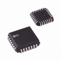
AD1671KP Analog Devices Inc, AD1671KP Datasheet - Page 12

AD1671KP
Manufacturer Part Number
AD1671KP
Description
IC ADC SNGL 12BIT 28PLCC
Manufacturer
Analog Devices Inc
Datasheet
1.AD1671JP.pdf
(16 pages)
Specifications of AD1671KP
Rohs Status
RoHS non-compliant
Number Of Bits
12
Sampling Rate (per Second)
1.25M
Data Interface
Parallel
Number Of Converters
2
Power Dissipation (max)
750mW
Voltage Supply Source
Analog and Digital, Dual ±
Operating Temperature
0°C ~ 70°C
Mounting Type
Surface Mount
Package / Case
28-LCC (J-Lead)
Available stocks
Company
Part Number
Manufacturer
Quantity
Price
Part Number:
AD1671KPZ
Manufacturer:
ADI/亚德诺
Quantity:
20 000
AD1671
APPLICATIONS
AD1671 TO ADSP-2100A
Figure 16 demonstrates the AD1671 to ADSP-2100A interface.
The 2100A with a clock frequency of 12.5 MHz can execute an
instruction in one 80 ns cycle. The AD1671 is configured to
perform continuous time sampling. The DAV output of the
AD1671 is asserted at the end of each conversion. DAV can be
used to latch the conversion result into the two 574 octal
D-latches. The falling edge of the sampling clock is used to
generate an interrupt (IRQ3) for the processor. Upon interrupt,
the ADSP-2100A starts a data memory read by providing an
address on the DMA bus. The decoded address generates OE
for the latches and the processor reads their output over the
DMA bus. The conversion result is read within a single proces-
sor cycle.
ADSP-
2100A
DMA0:13
DMA0:15
DMACK
DMRD
Figure 16. AD1671 to ADSP-2100A Interface
IRQ3
ADDRESS BUS
DECODE
+5V
16
DATA BUS
SAMPLING
CLOCK
8
8
OE
Q0:7
Q0:7
OE
574
574
D0:7
D0:3
D0:7
4
4
8
ENCODE
DAV
BIT1:12
AD1671
–12–
AD1671 TO ADSP-2101/2102
Figure 17 is identical to the 2100A interface except the sam-
pling clock is used to generate an interrupt (IRQ2) for the pro-
cessor. Upon interrupt the ADSP-2100A starts a data memory
read by providing an address on the address (A) bus. The de-
code address generates OE for the D-latches and the processor
reads their output over the Data (D) bus. Reading the conver-
sion result is thus completed within a single processor cycle.
ADSP-2101
Figure 17. AD1671 to ADSP-2101/ADSP-2102 Interface
A0:13
D0:15
IRQ2
RD
ADDRESS BUS
DECODE
16
DATA BUS
SAMPLING
CLOCK
8
8
OE
Q0:7
OE
Q0:7
574
574
D0:7
D0:3
D0:7
4
4
8
DAV
AD1671
BIT1:12
ENCODE
REV. B


