AD13280AF Analog Devices Inc, AD13280AF Datasheet
AD13280AF
Specifications of AD13280AF


Related parts for AD13280AF


AD13280AF Summary of contents
Page 1
FEATURES Dual 80 MSPS, minimum sample rate Channel-to-channel matching, ±1% gain error 90 dB channel-to-channel isolation DC-coupled signal conditioning 80 dB spurious-free dynamic range Selectable bipolar inputs (±1 V and ±0.5 V ranges) Integral single-pole, low-pass Nyquist filter Twos complement ...
Page 2
AD13280 TABLE OF CONTENTS Features .............................................................................................. 1 Applications....................................................................................... 1 Product Highlights ........................................................................... 1 Functional Block Diagram .............................................................. 1 Revision History ............................................................................... 2 General Description ......................................................................... 3 Specifications..................................................................................... 4 Timing Diagram ........................................................................... 6 Absolute Maximum Ratings............................................................ 7 Explanation of Test Levels ...
Page 3
GENERAL DESCRIPTION The AD13280 is a complete, dual-channel, signal processing solution that includes on-board amplifiers, references, ADCs, and output termination components to provide optimized system performance. The AD13280 has on-chip track-and-hold circuitry and uses an innovative multipass architecture to achieve ...
Page 4
AD13280 SPECIFICATIONS − +3.3 V; applies to each ADC with front-end amplifier, unless otherwise noted Table 1. Parameter RESOLUTION 1 DC ACCURACY No Missing Codes Offset Error Offset ...
Page 5
Parameter Analog Input @ 37 MHz SINAD 1, 7 Analog Input @ 10 MHz Analog Input @ 21 MHz Analog Input @ 37 MHz 1, 8 SPURIOUS-FREE DYNAMIC RANGE Analog Input @ 10 MHz Analog Input @ 21 MHz Analog ...
Page 6
AD13280 Parameter I (DV ) Current CC I (Total) Supply Current per Channel CC Power Dissipation (Total) Power Supply Rejection Ratio (PSRR) 1 All ac specifications tested by driving ENCODE and ENCODE differentially. Single-ended input: AMP-IN-x p-p, ...
Page 7
ABSOLUTE MAXIMUM RATINGS Table 2. Parameter 1 ELECTRICAL AV Voltage CC AV Voltage EE DV Voltage CC Analog Input Voltage Analog Input Current Digital Input Voltage (ENCODE) ENCODE, ENCODE Differential Voltage Digital Output Current 1 ENVIRONMENTAL Operating Temperature Range (Case) ...
Page 8
AD13280 PIN CONFIGURATION AND FUNCTION DESCRIPTIONS AGNDB AMP-IN-B-2 AMP-IN-B-1 AMP-OUT-B AGNDB AGNDB SHIELD AGNDA AGNDA AMP-OUT-A AMP-IN-A-1 AMP-IN-A-2 AGNDA Table 3. Pin Function Descriptions Pin No. Mnemonic Description 1, 35 SHIELD Internal Ground Shield Between Channels 10, ...
Page 9
Pin No. Mnemonic Description 54, 57, 60, 61, 67, 68 AGNDB B Channel Analog Ground. A and B grounds should be connected as close to the device as possible. 55 ENCODEB Encode Input. Conversion initiated on rising edge. 56 ENCODEB ...
Page 10
AD13280 TYPICAL PERFORMANCE CHARACTERISTICS 0 –10 –20 –30 –40 –50 –60 –70 3 – –90 –100 –110 –120 –130 FREQUENCY (MHz) Figure 4. Single Tone @ 5 MHz 0 –10 –20 –30 ...
Page 11
ENCODE = 80MSPS 2.5 DNL MAX = 0.688 CODES DNL MIN = 0.385 CODES 2.0 1.5 1.0 0.5 0 –0.5 –1.0 0 512 1024 1536 2048 2560 3072 Figure 10. Differential Nonlinearity 0 –1 ENCODE = 80MSPS –2 ROLL-OFF ...
Page 12
AD13280 TERMINOLOGY Analog Bandwidth The analog input frequency at which the spectral power of the fundamental frequency (as determined by the FFT analysis) is reduced by 3 dB. Aperture Delay The delay between a differential crossing of the ENCODEA signal ...
Page 13
INPUT AND OUTPUT STAGES AMP-IN-X-2 100 Ω AMP-IN-X-1 100Ω Figure 13. Single-Ended Input Stage DV CC CURRENT MIRROR V REF CURRENT MIRROR Figure 14. DR Digital Output Stage ENCODE TO AD8045 DV CC DROUT Rev Page 13 of ...
Page 14
AD13280 THEORY OF OPERATION The AD13280 is a high dynamic range 12-bit, 80 MHz pipeline delay (three pipelines) analog-to-digital converter (ADC). The custom analog input section provides input ranges p-p and 2 V p-p and input impedance ...
Page 15
APPLICATIONS INFORMATION ENCODING THE AD13280 The AD13280 encode signal must be a high quality, extremely low phase noise source to prevent degradation of performance. Maintaining 12-bit accuracy at 80 MSPS places a premium on encode clock phase noise. SNR performance ...
Page 16
AD13280 POWER SUPPLIES Care should be taken when selecting a power source. Linear supplies are strongly recommended. Switching supplies tend to have radiated components that may be received by the AD13280. Each of the power supply pins should be decoupled ...
Page 17
EVALUATION BOARD The AD13280 evaluation board (see Figure 20) is designed to provide optimal performance for evaluation of the AD13280 analog-to-digital converter. The board encompasses everything needed to ensure the highest level of performance for evaluating the AD13280. The board ...
Page 18
AD13280 J13 SMA J9 SMA J3 SMA AGNDA J4 SMA E51 AGNDA E69 AGNDA AGNDA AGNDA –5VAA 10 C9 AGNDA AGNDA 11 0.1µF AV AGENDA 12 AV +5VAA 13 C34 C35 AGNDA AGNDA 0.1µF 0.1µF 14 ENCODEA ENCODEA 15 ENCODEA ...
Page 19
U8 R47 LE2 OE2 0Ω 115 O15 26 23 114 O14 R48 22 27 DGNDA GND GND 0Ω NC0A 113 O13 29 20 DGNDA NC1A 112 O12 30 19 DUT_3.3VDA VCC VCC 18 31 (LSB) D0A ...
Page 20
AD13280 +5VAA J5 ENCODE C1 0.1µF SMA R1 AGNDA 50Ω AGNDA DGNDA J12 R55 C2 SMA 33kΩ 0.1µF 1 R41 NC VCC 25Ω AGNDA VBB VEE MC10EP16 CONNECT +5VAB J10 C22 ...
Page 21
Figure 24. Top Silk Figure 25. Top Layer Rev Page AD13280 ...
Page 22
AD13280 Figure 26. GND1 Figure 27. GND2 Rev Page ...
Page 23
Figure 28. Bottom Silk Figure 29. Bottom Layer Rev Page AD13280 ...
Page 24
AD13280 BILL OF MATERIALS LIST FOR EVALUATION BOARD Table 4. Component Name Qty Reference 2 74LCX16374MTD U7 AD13280AZ U1 2 ADP3330 U5 BJACK BJ1 to BJ10 2 BRES0805 R41, R53 4 BRES0805 R38, R39, R55, R56 ...
Page 25
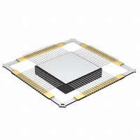
OUTLINE DIMENSIONS 0.035 (0.889) MAX DETAIL A TOE DOWN ANGLE 0–8 DEGREES 0.010 (0.254) 30° 0.050 (1.27) 0.020 (0.508) DETAIL A ROTATED 90° CCW 0.010 (0.25) 0.008 (0.20) 0.007 (0.18) 0.235 (5.97) MAX Figure 30. 68-Lead Ceramic Leaded Chip Carrier ...
Page 26
... AD13280 ORDERING GUIDE Model Temperature Range AD13280AZ 2 −25°C to +85°C AD13280AF −25°C to +85°C AD13280/PCB 1 Referenced temperature is case temperature package indicator; the part is not RoHS compliant. 1 Package Description 68-Lead Ceramic Leaded Chip Carrier [CLCC] 68-Lead Ceramic Leaded Chip Carrier with Nonconductive Tie-Bar [CLCC] Evaluation Board with AD13280AZ Rev ...
Page 27
NOTES Rev Page AD13280 ...
Page 28
AD13280 NOTES ©2002–2008 Analog Devices, Inc. All rights reserved. Trademarks and registered trademarks are the property of their respective owners. D02386–0–4/08(C) Rev Page ...