AD13280AF Analog Devices Inc, AD13280AF Datasheet - Page 16
AD13280AF
Manufacturer Part Number
AD13280AF
Description
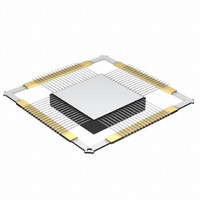
IC ADC 12BIT 68CLCC
Manufacturer
Analog Devices Inc
Datasheet
1.AD13280AF.pdf
(28 pages)
Specifications of AD13280AF
Rohs Status
RoHS non-compliant
Number Of Bits
12
Sampling Rate (per Second)
80M
Data Interface
Parallel
Number Of Converters
2
Power Dissipation (max)
4.3W
Voltage Supply Source
Analog and Digital, Dual ±
Operating Temperature
-25°C ~ 85°C
Mounting Type
Surface Mount
Package / Case
68-CLCC
For Use With
AD13280/PCB - KIT EVAL PCB FOR AD13280


AD13280
POWER SUPPLIES
Care should be taken when selecting a power source. Linear
supplies are strongly recommended. Switching supplies tend
to have radiated components that may be received by the
AD13280. Each of the power supply pins should be decoupled
as close as possible to the package using 0.1 μF chip capacitors.
The AD13280 has separate digital and analog power supply
pins. The analog supplies are denoted AV
supply pins are denoted DV
separate power supplies because the fast digital output swings
can couple switching current back into the analog supplies.
Note that AV
specified for DV
digital ASICs.
CC
must be held within 5% of 5 V. The AD13280 is
CC
= 3.3 V because this is a common supply for
CC
. AV
CC
and DV
CC
, and the digital
CC
should be
Rev. C | Page 16 of 28
OUTPUT LOADING
Care must be taken when designing the data receivers for the
AD13280. The digital outputs drive an internal series resistor
(for example, 100 Ω) followed by a gate like 75LCX574. To
minimize capacitive loading, there should be only one gate on
each output pin. An example of this is shown in the evaluation
board schematic (see Figure 20). The digital outputs of the
AD13280 have a constant output slew rate of 1 V/ns.
A typical CMOS gate combined with a PCB trace has a load of
approximately 10 pF. Therefore, as each bit switches, 10 mA
(10 pF × 1 V ÷ 1 ns) of dynamic current per bit flows in or out
of the device. A full-scale transition can cause up to 120 mA
(12 bits × 10 mA/bit) of transient current through the output
stages. These switching currents are confined between ground
and the DVCC pin. Standard TTL gates should be avoided
because they can appreciably add to the dynamic switching
currents of the AD13280. It should also be noted that extra
capacitive loading increases output timing and invalidates
timing specifications. Digital output timing is guaranteed with
10 pF loads.
Related parts for AD13280AF
Image
Part Number
Description
Manufacturer
Datasheet
Request
R

Part Number:
Description:
±1.7g Dual-Axis IMEMS Accelerometer Evaluation Board
Manufacturer:
Analog Devices Inc
Datasheet:

Part Number:
Description:
Inertial Sensor Evaluation System
Manufacturer:
Analog Devices Inc
Datasheet:
Part Number:
Description:
Manufacturer:
Analog Devices Inc
Datasheet:
Part Number:
Description:
Manufacturer:
Analog Devices Inc
Datasheet:
Part Number:
Description:
Manufacturer:
Analog Devices Inc
Datasheet:
Part Number:
Description:
Manufacturer:
Analog Devices Inc
Datasheet:
Part Number:
Description:
Manufacturer:
Analog Devices Inc
Datasheet:
Part Number:
Description:
Manufacturer:
Analog Devices Inc
Datasheet:
Part Number:
Description:
Manufacturer:
Analog Devices Inc
Datasheet:
Part Number:
Description:
Manufacturer:
Analog Devices Inc
Datasheet:
Part Number:
Description:
Manufacturer:
Analog Devices Inc
Datasheet:
Part Number:
Description:
Manufacturer:
Analog Devices Inc
Datasheet:
Part Number:
Description:
Manufacturer:
Analog Devices Inc
Datasheet: