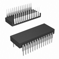
HI1-574AKD-5 Intersil, HI1-574AKD-5 Datasheet - Page 12

HI1-574AKD-5
Manufacturer Part Number
HI1-574AKD-5
Description
IC ADC 12BIT 40KSPS 1CH 28-SBDIP
Manufacturer
Intersil
Datasheet
1.HI3-574AKN-5Z.pdf
(18 pages)
Specifications of HI1-574AKD-5
Number Of Bits
12
Sampling Rate (per Second)
40k
Data Interface
Parallel
Number Of Converters
1
Power Dissipation (max)
720mW
Voltage Supply Source
Dual ±
Operating Temperature
0°C ~ 75°C
Mounting Type
Through Hole
Package / Case
28-CDIP (0.600", 15.24mm)
Lead Free Status / RoHS Status
Lead free / RoHS Compliant
Available stocks
Company
Part Number
Manufacturer
Quantity
Price
Company:
Part Number:
HI1-574AKD-5
Manufacturer:
Intersil
Quantity:
352
Part Number:
HI1-574AKD-5
Manufacturer:
HAR
Quantity:
20 000
required, either or both pots may be replaced by a 50Ω, 1%
metal film resistor.
Connect the Analog signal to pin 13 for a ±5V range, or to
pin 14 for a ±10V range. Calibration of offset and gain is
similar to that for the unipolar ranges as discussed above.
First apply a DC input voltage
scale (i.e., -4.9988V for the ±5V range, or -9.9976V for the
±10V range). Adjust the offset potentiometer R1 for flicker
between output codes 0000 0000 0000 and 0000 0000
0001. Next, apply a DC input voltage 1
positive full scale (+4.9963V for ±5V range; +9.9927V for
±10V range). Adjust the Gain potentiometer R2 for flicker
between codes 1111 1111 1110 and 1111 1111 1111.
NOTE: The 100Ω potentiometer R2 provides Gain Adjust for the 10V
and 20V ranges. In some applications, a full scale of 10.24V (LSB
equals 2.5mV) or 20.48V (LSB equals 5.0mV) is more convenient.
For these, replace R2 by a 50Ω, 1% metal film resistor. Then, to pro-
vide Gain Adjust for the 10.24V range, add a 200Ω potentiometer in
series with pin 13. For the 20.48V range, add a 500Ω potentiometer
in series with pin 14.
Controlling the HI-X74A
The HI-X74A includes logic for direct interface to most
microprocessor systems. The processor may take full
control of each conversion, or the converter may operate in
the “stand-alone” mode, controlled only by the R/C input.
Full control consists of selecting an 8-bit or 12-bit
conversion cycle, initiating the conversion, and reading the
output data when ready-choosing either 12 bits at once or 8
followed by 4, in a left-justified format. The five control
inputs are all TTL/CMOS-compatible: (12/8, CS, A
and CE). Table 3 illustrates the use of these inputs in
controlling the converter’s operations. Also, a simplified
schematic of the internal control logic is shown in Figure 6.
“Stand-Alone Operation”
The simplest control interface calls for a single control line
connected to R/C. Also, CE and 12/8 are wired high, CS and
A
12 bits each.
The R/C signal may have any duty cycle within (and
including) the extremes shown in Figures 7 and 8. In
general, data may be read when R/C is high unless STS is
also high, indicating a conversion is in progress. Timing
parameters particular to this mode of operation are listed in
Tables 1 and 2.
O
are wired low, and the output data appears in words of
12
1
/
2
LSB above negative full
1
/
2
LSBs below
O
HI-574A, HI-674A
, R/C
Conversion Length
A Convert Start transition (see Table 1) latches the state of
A
12 bits (A
read following an 8-bit conversion, the last three LSBs will
read ZERO and DB3 will read ONE. A
is also involved in enabling the output buffers (see ““Reading
the Output Data” on page 13). No other control inputs are
latched.
SYMBOL
Time is measured from 50% level of digital transitions. Tested with a
50pF and 3kΩ load.
Time is measured from 50% level of digital transitions. Tested with
a 50pF and 3kΩ load.
SYMBOL
CE
O
X
0
↑
↑
1
1
1
1
1
1
1
t
t
t
t
TABLE 3. TRUTH TABLE FOR HI-X74A CONTROL INPUTS
HDR
HRH
DDR
t
t
t
HRL
t
t
t
, which determines whether the conversion continues for
HDR
HRH
DDR
HRL
t
t
DS
HS
DS
HS
CS
X
1
0
0
↓
↓
0
0
0
0
0
TABLE 2. HI-674A STAND-ALONE MODE TIMING
TABLE 1. HI-574A STAND-ALONE MODE TIMING
O
Low R/C Pulse Width
STS Delay from R/C
Data Valid after R/C Low
STS Delay after Data Valid 300
High R/C Pulse Width
Data Access Time
R/C
Low R/C Pulse Width
STS Delay from R/C
Data Valid after R/C Low
STS Delay after Data
Valid
High R/C Pulse Width
Data Access Time
low) or stops with 8 bits (A
X
X
0
0
0
0
↓
↓
1
1
1
PARAMETER
PARAMETER
12/8
X
X
X
X
X
X
X
X
1
0
0
A
X
X
X
0
1
0
1
0
1
0
1
O
None
None
Initiate 12-bit conversion
Initiate 8-bit conversion
Initiate 12-bit conversion
Initiate 8-bit conversion
Initiate 12-bit conversion
Initiate 8-bit conversion
Enable 12-bit Output
Enable 8 MSBs Only
Enable 4 LSBs Plus 4 Trailing Zeroes
MIN
150
MIN
150
50
25
25
50
25
-
-
O
-
-
O
OPERATION
high). If all 12 bits are
is latched because it
TYP
TYP
-
-
-
-
-
-
-
-
-
-
-
-
MAX UNITS
MAX UNITS
1200
200
850
150
200
150
-
-
-
-
-
-
August 7, 2008
FN3096.6
ns
ns
ns
ns
ns
ns
ns
ns
ns
ns
ns
ns


