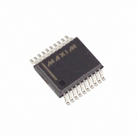
MAX152CAP+ Maxim Integrated Products, MAX152CAP+ Datasheet - Page 9

MAX152CAP+
Manufacturer Part Number
MAX152CAP+
Description
IC ADC 8BIT 1UA PWR-DWN 20-SSOP
Manufacturer
Maxim Integrated Products
Datasheet
1.MAX152CWP.pdf
(12 pages)
Specifications of MAX152CAP+
Number Of Bits
8
Sampling Rate (per Second)
400k
Data Interface
Parallel
Number Of Converters
3
Power Dissipation (max)
640mW
Voltage Supply Source
Dual ±
Operating Temperature
0°C ~ 70°C
Mounting Type
Surface Mount
Package / Case
20-SSOP
Lead Free Status / RoHS Status
Lead free / RoHS Compliant
Figures 7a-7c show some reference connections.
VREF+ and VREF- inputs set the full-scale and zero-
input voltages of the ADC. The voltage at VREF-
defines the input that produces an output code of all
zeros, and the voltage at VREF+ defines the input that
produces an output code of all ones.
The internal resistance from VREF+ to VREF- may be as
low as 1kΩ, and current will flow through it even when
the MAX152 is shut down. Figure 7d shows how an N-
channel MOSFET may be connected to VREF- to break
this path during power-down. The FET should have an
on resistance < 2Ω with a 3V gate drive.
Although VREF+ is frequently connected to V
circuit uses a low current, low-dropout, 2.5V voltage
reference – the MAX872. Since the MAX872 cannot
continuously furnish enough current for the reference
resistance, this circuit is intended for applications where
the MAX152 is normally in standby and is turned on in
order to make measurements at intervals greater than
20µs. The capacitor C1 connected to VREF+ is slowly
charged by the MAX872 during the standby period and
furnishes the reference current during the short measure-
ment period.
The 2.2µF value of C1 is chosen so that its voltage drops
by less than 1/2LSB during the conversion process.
Larger capacitors reduce the error still further. Use
ceramic or tantalum capacitors for C1.
When VREF- is switched, as in Figure 7d, a new conver-
sion can be initiated after waiting a time equal to the
power-up delay (t
nel FET.
A 4.7µF electrolytic in parallel with a 0.1µF ceramic
capacitor should be used to bypass V
These capacitors should have minimal lead length.
The reference inputs should be bypassed with 0.1µF
capacitors, as shown in Figures 7a-7c.
____________Analog Considerations
UP
_______________________________________________________________________________________
) plus the turn-on time of the N-chan-
+3V, 8-Bit ADC with 1µA Power-Down
Reference
Bypassing
DD
to GND.
DD
, this
Figure 8 shows the equivalent circuit of the converter
input. When the conversion starts and WR is low, V
connected to sixteen 0.6pF capacitors. During this acqui-
sition phase, the input capacitors charge to the input volt-
age through the resistance of the internal analog switches.
In addition, about 12pF of stray capacitance must be
charged. The input can be modeled as an equivalent RC
network (Figure 9). As source impedance increases, the
capacitors take longer to charge.
The typical 22pF input capacitance allows source resis-
tance as high as 2.2kΩ without setup problems. For larg-
er resistances, the acquisition time (t
Figure 8. Equivalent Input Circuit
Figure 9. RC Network Equivalent Input Model
V IN
R IN
V IN
1
V IN
R
C
MAX152
1
R ON
V IN
12pF
4k
10pF
P
) must be increased.
MAX152
Input Current
IN
is
9


