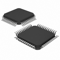
MAX1316ECM+T Maxim Integrated Products, MAX1316ECM+T Datasheet - Page 16

MAX1316ECM+T
Manufacturer Part Number
MAX1316ECM+T
Description
IC ADC 14BIT 8CH 2MSPS 48LQFP
Manufacturer
Maxim Integrated Products
Datasheet
1.MAX1318ECM.pdf
(27 pages)
Specifications of MAX1316ECM+T
Number Of Bits
14
Sampling Rate (per Second)
2M
Data Interface
Parallel
Number Of Converters
1
Voltage Supply Source
Single Supply
Operating Temperature
-40°C ~ 85°C
Mounting Type
Surface Mount
Package / Case
48-LQFP
Lead Free Status / RoHS Status
Lead free / RoHS Compliant
8-/4-/2-Channel, 14-Bit, Simultaneous-Sampling ADCs
with ±10V, ±5V, and 0 to +5V Analog Input Ranges
To write to the configuration register, pull CS and WR
low, load bits D0–D7 onto the parallel bus, and force
WR high. The data are latched on the rising edge of
WR (Figure 4). It is possible to write to the configuration
register at any point during the conversion sequence;
however, it is not active until the next convert-start sig-
nal. At power-up, write to the configuration register to
select the active channels before beginning a conver-
sion. Shutdown does not change the configuration reg-
ister. See the Shutdown Mode and the ALLON sections
for information about using the configuration register for
power saving.
To start a conversion using internal-clock mode, pull
CONVST low for at least the acquisition time (t
T/H acquires the signal while CONVST is low, and con-
version begins on the rising edge of CONVST. An end-
of-conversion signal (EOC) pulses low when the first
result becomes available, and for each subsequent
result until the end of the conversion cycle. The end-of-
last-conversion signal (EOLC) goes low when the last
conversion result is available (Figures 5, 6, and 7).
To start a conversion using external-clock mode, pull
CONVST low for at least the acquisition time (t
acquires the signal while CONVST is low, and conversion
begins on the rising edge of CONVST. Apply an external
clock to CLK. To avoid T/H droop degrading the sampled
analog input signals, the first clock pulse should occur
within 10µs from the rising edge of CONVST, and have a
minimum clock frequency of 100kHz. The first conversion
result is available for read on the rising edge of the 17th
clock cycle, and subsequent conversions after every third
clock cycle thereafter (Figures 5, 6, and 7).
Table 2. Configuration Register
NA = Not applicable.
16
PART NO.
MAX1316
MAX1320
MAX1324
MAX1317
MAX1321
MAX1325
MAX1318
MAX1322
MAX1326
______________________________________________________________________________________
STATE
OFF
OFF
OFF
ON
ON
ON
D0/CH0
Starting a Conversion
1
0
1
0
1
0
D1/CH1
1
0
1
0
1
0
1
). The T/H
1
D2/CH2
). The
NA
NA
1
0
1
0
D3/CH3
In both internal- and external-clock modes, CONVST
must be held high until the last conversion result is
read. For best operation, the rising edge of CONVST
must be a clean, high-speed, low-jitter digital signal.
Table 3 shows the total throughput as a function of the
clock frequency and the number of channels selected
for conversion. The calculations use the nominal speed
of the internal clock (10MHz) and a 200ns CONVST
pulse width.
Figure 4. Write Timing
NA
NA
BIT/CHANNEL
1
0
1
0
D0–D7
WR
RD
CS
D4/CH4
t
6
NA
NA
NA
NA
1
0
D5/CH5
t
NA
NA
NA
NA
14
1
0
t
t
2
5
DATA-IN
D6/CH6
NA
NA
NA
NA
1
0
t
t
7
15
D7/CH7
NA
NA
NA
NA
1
0


