MAX105ECS+ Maxim Integrated Products, MAX105ECS+ Datasheet - Page 11
MAX105ECS+
Manufacturer Part Number
MAX105ECS+
Description
IC ADC 6BIT 800MSPS DL 80TQFP
Manufacturer
Maxim Integrated Products
Datasheet
1.MAX105ECS.pdf
(21 pages)
Specifications of MAX105ECS+
Number Of Bits
6
Sampling Rate (per Second)
800M
Data Interface
Parallel
Number Of Converters
2
Power Dissipation (max)
2.6W
Voltage Supply Source
Analog and Digital
Operating Temperature
-40°C ~ 85°C
Mounting Type
Surface Mount
Package / Case
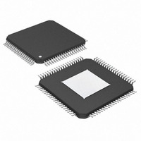
80-TQFP Exposed Pad, 80-eTQFP, 80-HTQFP, 80-VQFP
Number Of Adc Inputs
2
Conversion Rate
800 MSPs
Resolution
6 bit
Snr
37 dB
Voltage Reference
2.5 V
Supply Voltage (max)
3.6 V
Supply Voltage (min)
3 V
Maximum Power Dissipation
3.5 W
Maximum Operating Temperature
+ 85 C
Mounting Style
SMD/SMT
Input Voltage
3.3 V
Minimum Operating Temperature
- 40 C
Lead Free Status / RoHS Status
Lead free / RoHS Compliant


The MAX105 is a dual, +5V, 6-bit, 800Msps flash ana-
log-to-digital converter (ADC), designed for high-
speed, high-bandwidth I&Q digitizing. Each ADC
(Figure 1) employs a fully differential, wide bandwidth
input stage, 6-bit quantizers and a unique encoding
scheme to limit metastable states to typically one error
per 10
mum of 1LSB. An integrated 6:12 output demultiplexer
simplifies interfacing to the part by reducing the output
data rate to one-half the sampling clock rate. The
MAX105 outputs data in LVDS two’s complement for-
mat.
When clocked at 800Msps, the MAX105 provides a typ-
ical signal-to-noise plus distortion (SINAD) of 36.4dB
with a 200MHz input tone. The analog input of the
MAX105 is designed for differential or single-ended use
with a ±400mV full-scale input range. In addition, the
65, 72
66, 71
PIN
62
63
64
67
68
69
70
73
74
75
76
77
78
79
80
16
clock cycles, with no error exceeding a maxi-
OGNDI
NAME
OV
A2I+
A3I+
A4I+
A5I+
P2I+
P3I+
P4I+
P5I+
A2I-
P3I-
A3I-
P4I-
A4I-
P5I-
A5I-
______________________________________________________________________________________
CC
Dual, 6-Bit, 800Msps ADC with On-Chip,
I
Detailed Description
Primary Output Data Bit 2, I-Channel
Complementary Auxiliary Output Data Bit 2, I-Channel
Auxiliary Output Data Bit 2, I-Channel
I-Channel Outputs, Digital Supply. Supplies I-channel output drivers and DREADY circuit. Bypass to
OGND with 0.01µF in parallel with 47pF for proper operation.
I-Channel Outputs, Digital Ground. Connect to designated digital ground (OGND) on PC board
for proper operation.
Complementary Primary Output Data Bit 3, I-Channel
Primary Output Data Bit 3, I-Channel
Complementary Auxiliary Output Data Bit 3, I-Channel
Auxiliary Output Data Bit 3, I-Channel
Complementary Primary Output Data Bit 4, I-Channel
Primary Output Data Bit 4, I-Channel
Complementary Auxiliary Output Data Bit 4, I-Channel
Auxiliary Output Data Bit 4, I-Channel
Complementary Primary Output Data Bit 5, I-Channel
Primary Output Data Bit 5, I-Channel
Complementary Auxiliary Output Data Bit 5, I-Channel
Auxiliary Output Data Bit 5, I-Channel
Wideband Input Amplifier
MAX105 features an on-board +2.5V precision
bandgap reference, which is scaled to meet the analog
input full-scale range.
The MAX105 employs a flash or parallel architecture.
The key to this high-speed flash architecture is the use
of an innovative, high-performance comparator design.
Each quantizer and downstream logic translates the
comparator outputs into 6-bit, parallel codes in two’s
complement format and passes them on to the internal
6:12 demultiplexer. The demultiplexer enables the
ADCs to provide their output data at half the sampling
speed on primary and auxiliary ports. LVDS data is
available at speeds of up to 400MHz per output port.
As with all ADCs, if the input waveform is changing
rapidly during conversion, effective number of bits
(ENOB), signal-to-noise plus distortion (SINAD), and
FUNCTION
Pin Description (continued)
Input Amplifier Circuits
Principle of Operation
11
Related parts for MAX105ECS+
Image
Part Number
Description
Manufacturer
Datasheet
Request
R

Part Number:
Description:
MAX7528KCWPMaxim Integrated Products [CMOS Dual 8-Bit Buffered Multiplying DACs]
Manufacturer:
Maxim Integrated Products
Datasheet:
Part Number:
Description:
Single +5V, fully integrated, 1.25Gbps laser diode driver.
Manufacturer:
Maxim Integrated Products
Datasheet:
Part Number:
Description:
Single +5V, fully integrated, 155Mbps laser diode driver.
Manufacturer:
Maxim Integrated Products
Datasheet:
Part Number:
Description:
VRD11/VRD10, K8 Rev F 2/3/4-Phase PWM Controllers with Integrated Dual MOSFET Drivers
Manufacturer:
Maxim Integrated Products
Datasheet:
Part Number:
Description:
Highly Integrated Level 2 SMBus Battery Chargers
Manufacturer:
Maxim Integrated Products
Datasheet:
Part Number:
Description:
Current Monitor and Accumulator with Integrated Sense Resistor; ; Temperature Range: -40°C to +85°C
Manufacturer:
Maxim Integrated Products
Part Number:
Description:
TSSOP 14/A�/RS-485 Transceivers with Integrated 100O/120O Termination Resis
Manufacturer:
Maxim Integrated Products
Part Number:
Description:
TSSOP 14/A�/RS-485 Transceivers with Integrated 100O/120O Termination Resis
Manufacturer:
Maxim Integrated Products
Part Number:
Description:
QFN 16/A�/AC-DC and DC-DC Peak-Current-Mode Converters with Integrated Step
Manufacturer:
Maxim Integrated Products
Part Number:
Description:
TDFN/A/65V, 1A, 600KHZ, SYNCHRONOUS STEP-DOWN REGULATOR WITH INTEGRATED SWI
Manufacturer:
Maxim Integrated Products
Part Number:
Description:
Integrated Temperature Controller f
Manufacturer:
Maxim Integrated Products
Part Number:
Description:
SOT23-6/I�/45MHz to 650MHz, Integrated IF VCOs with Differential Output
Manufacturer:
Maxim Integrated Products
Part Number:
Description:
SOT23-6/I�/45MHz to 650MHz, Integrated IF VCOs with Differential Output
Manufacturer:
Maxim Integrated Products
Part Number:
Description:
EVALUATION KIT/2.4GHZ TO 2.5GHZ 802.11G/B RF TRANSCEIVER WITH INTEGRATED PA
Manufacturer:
Maxim Integrated Products
Part Number:
Description:
QFN/E/DUAL PCIE/SATA HIGH SPEED SWITCH WITH INTEGRATED BIAS RESISTOR
Manufacturer:
Maxim Integrated Products
Datasheet: