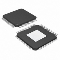
MAX105ECS+ Maxim Integrated Products, MAX105ECS+ Datasheet - Page 12

MAX105ECS+
Manufacturer Part Number
MAX105ECS+
Description
IC ADC 6BIT 800MSPS DL 80TQFP
Manufacturer
Maxim Integrated Products
Datasheet
1.MAX105ECS.pdf
(21 pages)
Specifications of MAX105ECS+
Number Of Bits
6
Sampling Rate (per Second)
800M
Data Interface
Parallel
Number Of Converters
2
Power Dissipation (max)
2.6W
Voltage Supply Source
Analog and Digital
Operating Temperature
-40°C ~ 85°C
Mounting Type
Surface Mount
Package / Case
80-TQFP Exposed Pad, 80-eTQFP, 80-HTQFP, 80-VQFP
Number Of Adc Inputs
2
Conversion Rate
800 MSPs
Resolution
6 bit
Snr
37 dB
Voltage Reference
2.5 V
Supply Voltage (max)
3.6 V
Supply Voltage (min)
3 V
Maximum Power Dissipation
3.5 W
Maximum Operating Temperature
+ 85 C
Mounting Style
SMD/SMT
Input Voltage
3.3 V
Minimum Operating Temperature
- 40 C
Lead Free Status / RoHS Status
Lead free / RoHS Compliant
signal-to-noise ratio (SNR) specifications will degrade.
The MAX105’s on-board, wide-bandwidth input ampli-
fiers (I&Q) reduce this effect significantly, allowing pre-
cise digitizing of fast analog data at high conversion
rates. The input amplifiers buffer the input signal and
allow a full-scale signal input range of ±400mV
(800mV
The MAX105 features an integrated, buffered +2.5V
precision bandgap reference. This reference is internal-
ly scaled to match the analog input range specification
of ±400mV. The data converter’s reference output
(REF) can source up to 500µA. REF should be buffered,
if used to supply external devices.
The MAX105 provides data in two’s complement format
to differential LVDS outputs. A simplified circuit
schematic of the LVDS output cells is shown in
2. All LVDS outputs are powered from separate I-chan-
nel OV
supplies, which may be operated at +3.3V ±10%. The
Dual, 6-Bit, 800Msps ADC with On-Chip,
Wideband Input Amplifier
Figure 1. MAX105 Flash Converter Architecture
12
______________________________________________________________________________________
INQ+
INQ-
INI+
INI-
CC
p-p
I and Q-channel OV
).
2kΩ
2kΩ
PRE-AMP
PRE-AMP
CM BUFFER
CM BUFFER
LVDS Digital Outputs
CC
Internal Reference
Q (Q-channel) power
REFERENCE
REF
Figure
REF
REF
Q ADC
I ADC
MAX105
Figure 2. Simplified LVDS Output Model
DOR
DOR+/DOR-
1:2
55Ω
DREADY+/DREADY-
DATA PORT
DATA PORT
DATA PORT
DATA PORT
AUXILIARY
AUXILIARY
PRIMARY
PRIMARY
P0Q-P5Q
A0Q-A5Q
OV
P0I-P5I
A0I-A5I
CC
I
55Ω
AV
CC
10kΩ
10kΩ
OV
MAX105
CC
I
OV
CC
P0I+/P0I-
P5I+/P5I-
A0I+/A0I-
A5I+/A5I-
CLK+
CLK-
P0Q+/P0Q-
P5Q+/P5Q-
A0Q+/A0Q-
A5Q+/A5Q-
I
P0I+ - P5I+
A0I+ - A5I+
P0I- - P5I-
A0I- - A5I-


