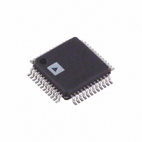
AD7677AST Analog Devices Inc, AD7677AST Datasheet

AD7677AST
Specifications of AD7677AST
Available stocks
Related parts for AD7677AST
AD7677AST Summary of contents
Page 1
FEATURES Throughput: 1 MSPS INL: 1 LSB Max ( 0.0015% of Full Scale) 16 Bits Resolution with No Missing Codes S/(N+D Typ @ 45 kHz THD: –110 dB Typ @ 45 kHz Differential Input Range: 2.5 V ...
Page 2
AD7677–SPECIFICATIONS Parameter RESOLUTION ANALOG INPUT Voltage Range Operating Input Voltage Analog Input CMRR Input Current Input Impedance THROUGHPUT SPEED Complete Cycle Throughput Rate Time Between Conversions Complete Cycle Throughput Rate Complete Cycle Throughput Rate DC ACCURACY Integral Linearity Error Differential ...
Page 3
Parameter POWER SUPPLIES Specified Performance AVDD DVDD OVDD 2 Operating Current AVDD 6 DVDD 6 OVDD 6 Power Dissipation 8 In Power-Down Mode 9 TEMPERATURE RANGE Specified Performance NOTES LSB means Least Significant Bit. With the ± 2.5 V input ...
Page 4
AD7677 TIMING SPECIFICATIONS Refer to Figures 11 and 12 Convert Pulsewidth Time Between Conversions (Warp Mode/Normal Mode/Impulse Mode) CNVST LOW to BUSY HIGH Delay BUSY HIGH All Modes Except in Master Serial Read after Convert Mode (Warp Mode/Normal Mode/Impulse Mode) ...
Page 5
... See Analog Input section. 3 Specification is for device in free air: 48-Lead LQFP: 4 Specification is for device in free air: LFCSP: = 26°C/W JA Model AD7677AST AD7677ASTRL AD7677ACP AD7677ACPRL 1 EVAL-AD7677CB EVAL-CONTROL BRD2 NOTES 1 This board can be used as a stand-alone evaluation board or in conjunction with the EVAL-CONTROL BRD2 for evaluation/ demonstration purposes ...
Page 6
AD7677 Pin No. Mnemonic Type Description 1 AGND P Analog Power Ground Pin 2 AVDD P Analog Power Pin. Nominally Connect 40–42, 44–48 4 BYTESWAP DI Parallel Mode Selection (8-bit/16-bit). When LOW, the LSB is ...
Page 7
Pin No. Mnemonic Type 19 DVDD P 20 DGND P 21 DATA[ SDOUT 22 DATA[9] DI/O or SCLK 23 DATA[10 SYNC 24 DATA[11 RDERROR 25–28 DATA[12:15 BUSY DO 30 DGND P RD ...
Page 8
AD7677 DEFINITION OF SPECIFICATIONS INTEGRAL NONLINEARITY ERROR (INL) Linearity error refers to the deviation of each individual code from a best-fit line drawn from “negative full scale” through “positive full scale.” The point used as “negative full scale” occurs 1/2 ...
Page 9
CODE TPC 1. Integral Nonlinearity vs. Code 9000 8287 8066 8000 7000 6000 5000 4000 3000 2000 1000 0000 7FFB 7FFC 7FFD 7FFE 7FFF ...
Page 10
AD7677 0 –20 –40 –60 –80 –100 –120 –140 –160 –180 0 100 200 300 FREQUENCY – kHz TPC 7. FFT Plot 100 95 SNR 100 FREQUENCY – kHz TPC 8. SNR, S/(N+D), ...
Page 11
TEMPERATURE – C TPC 13. Power-Down Operating Currents vs. Temperature CIRCUIT INFORMATION The AD7677 is a very fast, low power, single-supply, precise, 16-bit analog-to-digital converter (ADC). The AD7677 features ...
Page 12
AD7677 The Warp Mode allows the fastest conversion rate MSPS. However, in this mode, and this mode only, the full specified accu- racy is guaranteed only when the time between conversion does not exceed 1 ms. If ...
Page 13
AVDD IN+ IN– AGND Figure 6. Simplified Analog Input The diodes shown in Figure 6 provide ESD protection for the inputs. Care must be taken to ensure that the analog input sig- nal never exceeds the absolute ratings on these ...
Page 14
AD7677 For instance, a driver with an equivalent input noise of 2 nV/√Hz (like the AD8021) and configured as a buffer, thus with a noise gain of +1, the SNR degrades by only 0.07 dB with the filter in Figure ...
Page 15
CONVERSION CONTROL Figure 11 shows the detailed timing diagrams of the conversion process. The AD7677 is controlled by the signal CNVST, which initiates conversion. Once initiated, it cannot be restarted or aborted, even by the power-down input PD, until the ...
Page 16
AD7677 The BYTESWAP pin allows a glueless interface to an 8-bit bus. As shown in Figure 16, the LSB byte is output on D[7:0] and the MSB is output on D[15:8] when BYTESWAP is low. When BYTESWAP is high, the ...
Page 17
SERIAL INTERFACE The AD7677 is configured to use the serial interface when the SER/PAR is held high. The AD7677 outputs 16 bits of data, MSB first, on the SDOUT Pin. This data is synchronized with the 16 clock pulses provided ...
Page 18
AD7677 normally high or normally low when inactive. Figure 19 and Figure 20 show the detailed timing diagrams of these methods. While the AD7677 is performing a bit decision important that voltage transients not occur on digital input/output ...
Page 19
The AD7677 is configured for the internal clock mode (EXT/INT low) and acts, therefore, as the master device. The convert com- mand can be generated by either an external low jitter oscillator or, as shown FLAG output of ...
Page 20
AD7677 1.45 1.40 1.35 0.15 0.05 ROTATED 90 CCW BSC SQ PIN 1 INDICATOR 1.00 12 MAX 0.90 0.80 0.25 REF SEATING PLANE Revision History Location 7/02—Data Sheet changed from REV REV. A. Added 48-Lead LFCSP to FEATURES ...


