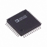
AD6600AST Analog Devices Inc, AD6600AST Datasheet - Page 19

AD6600AST
Manufacturer Part Number
AD6600AST
Description
IC ADC DUAL W/RSSI 44-LQFP
Manufacturer
Analog Devices Inc
Datasheet
1.AD6600ASTZ-REEL.pdf
(24 pages)
Specifications of AD6600AST
Rohs Status
RoHS non-compliant
Number Of Bits
11
Sampling Rate (per Second)
20M
Data Interface
Parallel
Number Of Converters
1
Power Dissipation (max)
976mW
Voltage Supply Source
Single Supply
Operating Temperature
-40°C ~ 85°C
Mounting Type
Surface Mount
Package / Case
44-LQFP
Available stocks
Company
Part Number
Manufacturer
Quantity
Price
Part Number:
AD6600AST
Manufacturer:
ADI/亚德诺
Quantity:
20 000
Company:
Part Number:
AD6600ASTREEL
Manufacturer:
INF
Quantity:
3 919
Company:
Part Number:
AD6600ASTZ
Manufacturer:
Analog Devices Inc
Quantity:
10 000
Part Number:
AD6600ASTZ
Manufacturer:
ADI/亚德诺
Quantity:
20 000
Company:
Part Number:
AD6600ASTZ-REEL
Manufacturer:
Analog Devices Inc
Quantity:
10 000
Figure 24 shows why settling is important for this circuit. If the
4×/8× amp does not settle (come out of clamp), the amplitude
presented to the ADC will be decreased. This results in decreased
gain when the filter capacitance is too high.
This explains why the total capacitance allowed for the external
filter varies depending on the clock rate (actually encode clock
high time). If the encode is 13 MSPS and the duty cycle is 50%,
the allowable settling time is 38.5 ns (1/2 of the encode time).
Our assumption is that the amp should be allowed to settle to
1/4 LSB in this time period. This has been proven with both
simulation and empirical analysis. If the settling is assumed to
be an RC circuit, then:
T = RC; t = time; n = number of bits
In this case, C
tance. R is nominally 315 Ω. The 8192 is (4 × 2048), which is
1/4 LSB of the converter (11 bits, 2048).
RESONANT
ENCODE
C
FILTER
TOTAL
GAIN STAGE
=
FROM
(
T
TOTAL
R l n
ENCODE
×
CLAMPED
HOLD
V
1
T
includes all parasitics and external capaci-
A
2
T
t
1
(
315
O
−
n
8192
× ×
=
−
=
×
=
2
=
1
A
l n
0 5
n
l n
e
A
.
× ×
AVCC
GND
t T
/
= −
)
( )
/
t
(
2
)
2
1
1
2
n
n
1
=
−
n
=
e
e
315
315
t T
t T
A
/
TRACK
SETTLING
/
(
)
1
Ω
38 5
ENCODE
−
×
e
.
t T
l n
/
ns
)
(
FILTER PORT
CLAMP
8192
RESONANT
)
HOLD
=
13 6
FLT
FLT
.
pF
So for settling purposes, with 13 MSPS encode and 50% duty
cycle, the maximum allowable capacitance for proper settling is
C
As stated above, this C
the board parasitics, and the AD6600 parasitics. The parasitics
of the AD6600 (lead, internal bond pad and internal connec-
tions) at FLT and FLT are 1.75 pF ± 0.35 pF (differential).
If the resistors are at maximum value (315 + 20%), the maxi-
mum allowable capacitance is C
cycle is less than 50%, the maximum allowable capacitance is
further decreased to allow for settling.
Power Supplies
Care should be taken when selecting a power source. Linear
supplies are strongly recommended. Switching supplies tend to
have radiated components that may be “received” by the AD6600.
Each of the power supply pins should be decoupled as closely to
the package as possible using 0.1 µF chip capacitors.
The AD6600 has separate digital and analog power supply pins.
The analog supplies are denoted AVCC and the digital supply
pins are denoted DVCC. Although analog and digital supplies
may be tied together, best performance is achieved when the
supplies are separate. This is because the fast digital output
swings can couple switching current back into the analog sup-
plies. Note that AVCC must be held within 5% of 5 Volts; how-
ever, the DVCC supply may be varied according to output
digital logic family. The AD6600 is specified for DVCC = 3.3 V
as this is a common supply for digital ASICS.
Output Loading
Care must be taken when designing the data receivers for the
AD6600. Note from the equivalent circuits shown earlier (see
Equivalent Circuits) that D[10:0] and RSSI[2:0] contain a
500 Ω output series resistor. To minimize capacitive loading,
there should only be one gate on each output pin. Extra capaci-
tive loading will increase output timing and invalidate timing
specifications. CLK2× and AB_OUT do not contain the output
series resistors. Testing for digital output timing is performed
with 10 pF loads.
Layout Information
The schematic of the evaluation board (Figure 25) represents a
typical implementation of the AD6600. A multilayer board is
recommended to achieve best results. It is highly recommended
that high quality, ceramic chip capacitors be used to decouple
each supply pin to ground directly at the device. The pinout of
the AD6600 facilitates ease of use in the implementation of high
frequency, high resolution design practices. All of the digital
outputs are segregated to two sides of the chip, with the inputs
on the opposite side for isolation purposes.
Care should be taken when routing the digital output traces. To
prevent coupling through the digital outputs into the analog
portion of the AD6600, minimal capacitive loading should be
placed on these outputs. It is recommended that a fanout of
only one be used for all AD6600 digital outputs.
The layout of the analog inputs and the external resonant filter
are critical. No digital traces must be routed near, under, or
above these portions of the circuit. The transformers used for
coupling into the analog inputs must be located as close as
possible to the analog inputs of the AD6600. The external reso-
nant filter components must be physically close to the filter-
input pins, yet separated from the analog inputs.
TOTAL
= 13.6 pF.
TOTAL
includes the external capacitors,
TOTAL
= 11.3 pF. If the duty
AD6600


