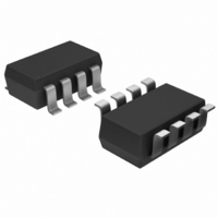
AD7453BRT-REEL7 Analog Devices Inc, AD7453BRT-REEL7 Datasheet

AD7453BRT-REEL7
Specifications of AD7453BRT-REEL7
Related parts for AD7453BRT-REEL7
AD7453BRT-REEL7 Summary of contents
Page 1
FEATURES Specified for Low power at max throughput rate: 3.3 mW max at 555 kSPS with 7.25 mW max at 555 kSPS with V DD Pseudo differential ...
Page 2
AD7453 TABLE OF CONTENTS Specifications..................................................................................... 3 Timing Specifications .................................................................. 5 Absolute Maximum Ratings............................................................ 6 ESD Caution.................................................................................. 6 Pin Configuration and Function Descriptions............................. 7 Terminology ...................................................................................... 8 AD7453–Typical Performance Characteristics ............................ 9 Circuit Information ........................................................................ 11 Converter Operation.................................................................. 11 ADC Transfer ...
Page 3
SPECIFICATIONS MHz SCLK S Table 1. Parameter DYNAMIC PERFORMANCE 2 Signal to Noise Ratio (SNR) 2 Signal to (Noise + Distortion) (SINAD) 2 Total Harmonic Distortion (THD) 2 ...
Page 4
AD7453 Parameter CONVERSION RATE Conversion Time 2 Track-and-Hold Acquisition Time Throughput Rate POWER REQUIREMENTS Normal Mode (Static) Normal Mode (Operational) Full Power-Down Mode Power Dissipation Normal Mode (Operational) Full Power-Down Mode 1 Temperature ranges ...
Page 5
TIMING SPECIFICATIONS Guaranteed by characterization. All input signals are specified with (10 level of 1.6 V. See Figure 2 and the Serial Interface section 2 5.25 ...
Page 6
AD7453 ABSOLUTE MAXIMUM RATINGS T = 25°C, unless otherwise noted. A Table 3. Parameter V to GND GND IN GND IN– Digital Input Voltage to GND Digital Output Voltage to GND V to GND REF ...
Page 7
PIN CONFIGURATION AND FUNCTION DESCRIPTIONS Table 4. Pin Function Descriptions Mnemonic Function V Reference Input for the AD7453. An external reference in the range 100 REF reference input is 2.5 V. This pin should be decoupled to ...
Page 8
AD7453 TERMINOLOGY Signal-to-(Noise + Distortion) Ratio The measured ratio of signal to (noise + distortion) at the output of the ADC. The signal is the rms amplitude of the fun- damental. Noise is the sum of all nonfundamental signals up ...
Page 9
AD7453–TYPICAL PERFORMANCE CHARACTERISTICS Default Conditions 25° 555 kSPS 4.75V 3. FREQUENCY (kHz) Figure 5. SINAD vs. Analog Input Frequency for Various ...
Page 10
AD7453 4.0 3.5 3.0 2.5 2.0 1.5 1.0 POSITIVE DNL 0.5 0 –0.5 NEGATIVE DNL –1 (V) REF Figure 11. Change in DNL vs. V REF POSITIVE INL 0 NEGATIVE ...
Page 11
CIRCUIT INFORMATION The AD7453 is a 12-bit, low power, single-supply, successive approximation analog-to-digital converter (ADC) with a pseudo differential analog input. It operates with a single 2 5.25 V power supply and is capable of throughput rates up ...
Page 12
AD7453 TYPICAL CONNECTION DIAGRAM Figure 17 shows a typical connection diagram for the AD7453. In this setup, the GND pin is connected to the analog ground plane of the system. The V pin is connected to the AD780, a REF ...
Page 13
When no amplifier is used to drive the analog input, the source impedance should be limited to low values. The maximum source impedance depends on the amount of total harmonic distortion (THD) that can be tolerated. The THD increases as ...
Page 14
AD7453 Sixteen serial clock cycles are required to perform a conversion and to access data from the AD7453. CS going low provides the first leading zero to be read in by the microcontroller or DSP. The remaining data is then ...
Page 15
MODES OF OPERATION The mode of operation of the AD7453 is selected by controlling the logic state of the CS signal during a conversion. There are two possible modes of operation, normal mode and power- down mode. The point at ...
Page 16
AD7453 POWER-UP TIME The power-up time of the AD7453 is typically 1 µs, which means that with any frequency of SCLK MHz, one dummy cycle is always sufficient to allow the device to power up. Once the ...
Page 17
POWER VS. THROUGHPUT RATE By using the power-down mode on the AD7453 when not con- verting, the average power consumption of the ADC decreases at lower throughput rates. Figure 27 shows how, as the through- put rate is reduced, the ...
Page 18
AD7453 The timer registers, for example, are loaded with a value that provides an interrupt at the required sample interval. When an interrupt is received, a value is transmitted with TFS/DT (ADC control word). The TFS is used to control ...
Page 19
APPLICATION HINTS Grounding and Layout The printed circuit board that houses the AD7453 should be designed so that the analog and digital sections are separated and confined to certain areas of the board. This facilitates the use of ground planes ...
Page 20
... BSC 0.15 MAX ORDERING GUIDE Model Temperature Range AD7453ART-REEL7 –40°C to +85°C AD7453BRT-R2 –40°C to +85°C AD7453BRT-REEL7 –40°C to +85°C 2 EVAL-AD7453CB 3 EVAL-CONTROL BRD2 1 Linearity error here refers to integral nonlinearity error. 2 This can be used as a standalone evaluation board or in conjunction with the evaluation board controller for evaluation/demonstration purposes. ...


