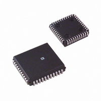
AD7885AAP-REEL Analog Devices Inc, AD7885AAP-REEL Datasheet - Page 9

AD7885AAP-REEL
Manufacturer Part Number
AD7885AAP-REEL
Description
IC ADC 16BIT SAMPLING HS 44-PLCC
Manufacturer
Analog Devices Inc
Datasheet
1.AD7885AAPZ.pdf
(16 pages)
Specifications of AD7885AAP-REEL
Rohs Status
RoHS non-compliant
Number Of Bits
16
Sampling Rate (per Second)
166k
Data Interface
Parallel
Number Of Converters
2
Power Dissipation (max)
325mW
Voltage Supply Source
Dual ±
Operating Temperature
-40°C ~ 85°C
Mounting Type
Surface Mount
Package / Case
44-PLCC
The required 3 V reference is derived from the AD780 and
buffered by the high speed amplifier A3 (AD845, AD817, or
equivalent). A4 is a unity gain inverter that provides the –3 V
negative reference. The gain setting resistors are on-chip and are
factory trimmed to ensure precise tracking of V
shows A3 and A4 as AD845s or AD817s. These have the ability to
respond to the rapidly changing reference input impedance.
CIRCUIT DESCRIPTION
Analog Input Section
The analog input section of the AD7884/AD7885 is shown in
Figure 7. It contains both the input signal conditioning and
sample-and-hold amplifier. Note that the analog input is truly
benign. When SW1
hold mode, SW1
R1 and R2, are always connected to either virtual ground or
true ground.
When the ± 3V
input section has a gain of –0.6 and transforms an input signal of
±5 V to the required ±3 V. When the ± 5V
are grounded, the input section has a gain of –1 and so the analog
input range is now ± 3 V. Resistors R4 and R5, at the amplifier
output, further condition the ± 3 V signal to be 0 V to –3 V. This
is the required input for the 9-bit A/D converter section.
With SW1
sample-and-hold is in the track mode). On the rising edge of
the CONVST pulse, SW1
holds the voltage on the output of A1. The sample-and-hold is
now in the hold mode. The aperture delay time for the sample-
and-hold is nominally 50 ns.
A/D Converter Section
The AD7884/AD7885 uses a two-pass flash technique in order
to achieve the required speed and resolution. When the CONVST
control input goes from low to high, the sample-and-hold ampli-
fier goes into the hold mode and a 0 V to –3 V signal is presented
to the input of the 9-bit ADC. The first phase of conversion
generates the 9 MSBs of the 16-bit result and transfers these to
the latch and ALU combination. They are also fed back to the
9 MSBs of the 16-bit DAC. The 7 LSBs of the DAC are
permanently loaded with 0s. The DAC output is subtracted from
the analog input with the result being amplified and offset in the
Residue Amplifier section.
REV. E
3V
3V
5V
5V
IN
IN
IN
IN
F
S
F
S
Figure 7. AD7884/AD7885 Analog Input Section
A
closed, the output of A1 follows the input (the
3k
5k
R1
R2
IN
SW1
B
S and ± 3V
is closed. This means that the input resistors,
A
B
goes open circuit to put the SHA into the
SW1
A
A
AMPLIFIER A2
goes open circuit and capacitor C1
IN
3k
TO RESIDUE
R3
F inputs are tied to 0 V, the
A1
C1
A1
R6
2k
IN
S and ±5V
4k
R4
REF+
V
REF–
R5
4k
. Figure 6
IN
F inputs
TO 9-BIT
ADC
–9–
The signal at the output of A2 is proportional to the error
between the first phase result and the actual analog input
signal and is digitized in the second conversion phase. This
second phase begins when the 16-bit DAC and the residue
error amplifier have both settled. First, SW2 is turned off and
SW3 is turned on. Then, the SHA section of the residue
amplifier goes into hold mode. Next SW2 is turned off and
SW3 is turned on. The 9-bit result is transferred to the output
latch and ALU. An error correction algorithm now compensates
for the offset inserted in the residue amplifier section and
errors introduced in the first pass conversion and combines both
results to give the 16-bit answer.
Timing and Control Section
Figure 9 shows the timing and control sequence for the AD7884/
AD7885. When the part receives a CONVST pulse, the con-
version begins. The input sample-and-hold goes into the hold
mode 50 ns after the rising edge of CONVST and BUSY goes
low. This is the first phase of conversion and takes 3.35 µs to
complete. The second phase of conversion begins when SW2 is
turned off and SW3 is turned on. The residue amplifier and
SHA section (A2 in Figure 8) goes into hold mode at this point
and allows the input sample-and-hold to go back into sample
mode. Thus, while the second phase of conversion is ongoing,
the input sample-and-hold is also acquiring the input signal for
the next conversion. This overlap between conversion and
acquisition allows throughput rates of 166 kSPS to be achieved.
INPUT
CONVST
FROM INPUT
SHA
3V SIGNAL
BUSY
SAMPLE
FIRST PHASE OF CONVERSION
SHA
HOLD
FIRST 9-BIT CONVERSION
DAC SETTLING TIME
RESIDUE AMPLIFIER
SETTLING TIME
Figure 9. Timing and Control Sequence
2k
Figure 8. A/D Converter Section
R6
V
REF+
RESIDUE AMP
+ SHA
4k
R4
F
4k
V
A2
R5
ACCURATE
REF+
+3V
FIRST PHASE
16-BIT
DAC
2k
S V
0 TO –3V
V
R7
3.5 s
REF–
–3V
INV
SW3
2k
R8
SW2
AD7884/AD7885
V
9
REF–
SECOND PHASE OF CONVERSION
SECOND 9-BIT CONVERSION
ERROR CORRECTION
OUTPUT LATCH UPDATE
9-BIT
ADC
SECOND
PHASE
1.8 s
TACQ
2.5 s
9
9
LATCH
ALU
+
16


