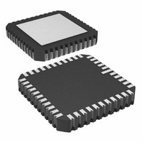
AD872AJE Analog Devices Inc, AD872AJE Datasheet - Page 13

AD872AJE
Manufacturer Part Number
AD872AJE
Description
IC ADC 12BIT 10MSPS 44-CLCC
Manufacturer
Analog Devices Inc
Datasheet
1.AD872AJD.pdf
(20 pages)
Specifications of AD872AJE
Rohs Status
RoHS non-compliant
Number Of Bits
12
Sampling Rate (per Second)
10M
Data Interface
Parallel
Number Of Converters
7
Power Dissipation (max)
1.3W
Voltage Supply Source
Analog and Digital, Dual ±
Operating Temperature
0°C ~ 70°C
Mounting Type
Surface Mount
Package / Case
44-CLCC
Available stocks
Company
Part Number
Manufacturer
Quantity
Price
condition or an out-of-range low condition. Note that if the in-
put is driven beyond +1.5 V, the digital outputs may not stay at
+FS, but may actually fold back to midscale.
The AD872A’s CMOS digital output drivers are sized to pro-
vide sufficient output current to drive a wide variety of logic
families. However, large drive currents tend to cause glitches on
the supplies and may affect S/(N+D) performance. Applications
requiring the AD872A to drive large capacitive loads or large
fanout may require additional decoupling capacitors on DRV
and DV
be used.
THREE-STATE OUTPUTS
The 44-terminal surface mount AD872A offers three-state out-
puts. The digital outputs can be placed into a three-state mode
by pulling the OUTPUT ENABLE (OEN) pin LOW. Note that
this function is not intended to be used to pull the AD872A on
and off a bus at 10 MHz. Rather, it is intended to allow the ADC
to be pulled off the bus for evaluation or test modes. Also, to
avoid corruption of the sampled analog signal during conversion
(3 clock cycles), it is highly recommended that the AD872A be
placed on the bus prior to the first sampling.
For timing budgetary purposes, the typical access and float de-
lay times for the AD872A are 50 ns.
CLOCK INPUT
The AD872A internal timing control uses the two edges of the
clock input to generate a variety of internal timing signals. The
optimal clock input should have a 50% duty cycle; however,
sensitivity to duty cycle is significantly reduced for clock rates of
less than 10 megasamples per second.
Due to the nature of on-chip compensation circuitry, the duty
cycle should be maintained between 40% and 60% even for
clock rates less than 10 MSPS. One way to realize a 50% duty
cycle clock is to divide down a clock of higher frequency, as
shown in Figure 26.
REV. A
OUTPUT
Figure 25. Three-State Output Timing Diagram
DATA
OEN
DD
. In extreme cases, external buffers or latches could
Figure 26. Divide-by-Two Clock Circuit
20MHz
THREE-STATE
D
t
DD
74XX74
+5V
+5V
R
S
Q
Q
ACTIVE
CLK
t
HL
DD
–13–
In this case, a 20 MHz clock is divided by 2 to produce the
10 MHz clock input for the AD872A. In this configuration, the
duty cycle of the 20 MHz clock is irrelevant.
The input circuitry for the CLKIN pin is designed to accom-
modate both TTL and CMOS inputs. The quality of the logic
input, particularly the rising edge, is critical in realizing the best
possible jitter performance for the part: the faster the rising
edge, the better the jitter performance.
As a result, careful selection of the logic family for the clock
driver, as well as the fanout and capacitive load on the clock
line, is important. Jitter-induced errors become more pro-
nounced at higher frequency, large amplitude inputs, where the
input slew rate is greatest.
The AD872A is designed to support a sampling rate of 10
MSPS; running at slightly faster clock rates may be possible,
although at reduced performance levels. Conversely, some slight
performance improvements might be realized by clocking the
AD872A at slower clock rates. Figure 27 presents the S/(N+D)
vs. clock frequency for a 1 MHz analog input.
The power dissipated by the correction logic and output buffers
is largely proportional to the clock frequency; running at re-
duced clock rates provides a slight reduction in power consump-
tion. Figure 28 illustrates this tradeoff.
Figure 28. Typical Power Dissipation vs. Clock Frequency
Figure 27. Typical S/(N+D) vs. Clock Frequency,
f
IN
1.09
1.08
1.07
1.06
1.05
1.04
75
70
65
60
55
50
= 1 MHz, Full-Scale Input
0
0
2
2
4
4
6
6
FREQUENCY – MHz
FREQUENCY – MHz
8
8
10
10
12
12
14
14
AD872A
16
16
18
18
20
20


