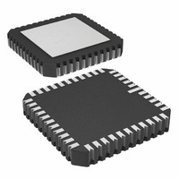
AD872AJE Analog Devices Inc, AD872AJE Datasheet - Page 15

AD872AJE
Manufacturer Part Number
AD872AJE
Description
IC ADC 12BIT 10MSPS 44-CLCC
Manufacturer
Analog Devices Inc
Datasheet
1.AD872AJD.pdf
(20 pages)
Specifications of AD872AJE
Rohs Status
RoHS non-compliant
Number Of Bits
12
Sampling Rate (per Second)
10M
Data Interface
Parallel
Number Of Converters
7
Power Dissipation (max)
1.3W
Voltage Supply Source
Analog and Digital, Dual ±
Operating Temperature
0°C ~ 70°C
Mounting Type
Surface Mount
Package / Case
44-CLCC
Available stocks
Company
Part Number
Manufacturer
Quantity
Price
Figure 32 shows how a dc offset can be applied using the
AD568 12-bit, high speed digital-to-analog converter (DAC).
This circuit can be used for applications requiring offset adjust-
ments on every clock cycle. The AD568 connection scheme is
used to provide a –0.512 V to +0.512 V output range. The off-
set voltage must be stable on the rising edge of the AD872A
clock input.
UNDERSAMPLING USING THE AD872A AND AD9100
The AD872A’s on-chip THA optimizes transient response while
maintaining low noise performance. For super-Nyquist (under-
sampling) applications it may be necessary to use an external
THA with fast track-mode slew rate and hold mode settling
time. An excellent choice for this application is the AD9100, an
ultrahigh speed track-and-hold amplifier.
REV. A
DIGITAL
OFFSET
WORD
Figure 32. Offset Correction Using the AD568
8
4
574
574
HC
HC
74
74
CLOCK 1
I N
+V
–V
ALL CAPACITORS ARE 0.01 F
(LOW INDUCTANCE - DECOUPLING)
UNLESS OTHERWISE NOTED.
S
S
8
4
= 5.0V
= –5.2V
R
T
AD568
REF COM
t
S
= 17ns
10
ACOM
LCOM
9
IBPO
IOUT
+V
1
CLOCK 2
CLOCK 1
RL
S
96685
Figure 33. Undersampling Using the AD872A and AD9100
AD
5
–V
4
V
8
7
S
IN
510
Q
Q
–V
S
V
–V
I N
S
1
2
510
R
T
AD872A
V
V
INA
INB
19
18
10
13
11
17
12
4
2
3
8
AD9100
t
S
T = 200ns
10 F
–15–
T = 200ns
14
16
15
1
20
6
5
7
In order to maximize the spurious free dynamic range of the
circuit in Figure 33 it is advantageous to present a small signal
to the input of the AD9100 and then amplify the output to the
AD872A’s full-scale input range. This can be accomplished with
a low distortion, wide bandwidth amplifier such as the AD9617.
The circuit uses a gain of 3.5 to optimize S/(N+D).
For small scale input signals (–20 dB, –40 dB), the AD872A
performs better without the track-and-hold because slew-
limiting effects are no longer dominant. To gain the advantages
of the added track-and-hold, it is important to give the AD872A
a full-scale input.
An alternative to the configuration presented above is to use the
AD9101 track-and-hold amplifier. The AD9101 provides a
built-in post amplifier with a gain of 4, providing excellent ac
characteristics in conjunction with a high level of integration.
As illustrated in Figure 33, it is necessary to skew the AD872A
sample clock and the AD9100 sample/hold control. Clock skew
(t
into hold mode and ending at the moment the AD872A samples.
The AD872A samples on the rising edge of the sample clock,
and the AD9100 samples on the falling edge of the sample/hold
control. The choice of t
time of the AD9100. The droop rate of the AD9100 must also
be taken into consideration. Using these values, the ideal t
17 ns. When choosing clock sources, it is extremely important
that the front end track-and-hold sample/hold control is given a
very low jitter clock source. This is not as crucial for the
AD872A sample clock, because it is sampling a dc signal.
+V
S
S
) is defined as the time starting at the AD9100’s transition
–V
S
127
10 F
2
3
4
–5V
+5V
7
9617
AD
0.1 F
8*
5*
0.1 F
442
3.3 F
3.3 F
6
0.1 F
0.1 F
S
is primarily determined by the settling
* OPTIONAL, SEE
AD9617 DATASHEET
A
+5V
0V
+1V
–1V
I N
AD872A
CLOCK 2
EB
IN
AD872A
S
is


