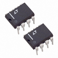
LTC1291DCN8#PBF Linear Technology, LTC1291DCN8#PBF Datasheet

LTC1291DCN8#PBF
Specifications of LTC1291DCN8#PBF
Available stocks
Related parts for LTC1291DCN8#PBF
LTC1291DCN8#PBF Summary of contents
Page 1
... Given the accuracy, ease of use and small package size, this device is well suited for digitizing analog signals in remote applications where minimum number of inter- connects, small physical size, and low power consump- tion are important. , LTC and LT are registered trademarks of Linear Technology Corporation. TM LTCMOS is a trademark of Linear Technology Corporation 22 F ...
Page 2
LTC1291 BSOLUTE (Notes 1 and 2) Supply Voltage ( GND .................................. 12V CC Voltage Analog Inputs ............................ –0. Digital Inputs ........................................ –0.3V to 12V Digital Outputs .......................... –0.3V to ...
Page 3
AC CHARACTERISTICS otherwise specifications are (Note 3) A SYMBOL PARAMETER t Delay Time Hi-Z dis OUT t Delay Time, CLK to D Enabled en OUT t Hold Time, D after CLK hDI ...
Page 4
LTC1291 W U TYPICAL PERFOR A Supply Current vs Supply Voltage 10 CLK = 1MHz SUPPLY VOLTAGE (V) 1291 G01 Change in Linearity vs Supply Voltage 0.5 0.4 ...
Page 5
W U TYPICAL PERFOR A D Delay Time vs Temperature OUT 250 200 MSB-FIRST DATA 150 100 LSB-FIRST DATA 50 0 –50 – 100 125 AMBIENT TEMPERATURE ( C) 1291 G10 Sample-and-Hold ...
Page 6
LTC1291 W BLOCK I D AGRA REF INPUT 5 SHIFT D IN REGISTER 2 CH0 ANALOG 3 INPUT MUX CH1 4 GND TEST CIRCUITS Load Circuit for dDO 1. OUT ...
Page 7
TEST CIRCUITS Voltage Waveforms for D Rise and Fall Times, t OUT D OUT START IN CLK 1 D OUT PPLICATI S I FOR ATIO The LTC1291 is a data acquisition component ...
Page 8
LTC1291 PPLICATI S I FOR ATIO DATA ( Data transfer is initiated by a falling chip IN OUT select (CS) signal. After CS falls, the LTC1291 looks for a start bit. After the start ...
Page 9
PPLICATI S I FOR ATIO Input Data Word The 4-bit data word is clocked into the D edge of the clock after chip select goes low and the start bit has been recognized. Further inputs on ...
Page 10
LTC1291 PPLICATI S I FOR ATIO Output Code The LTC1291 performs a unipolar conversion. The follow- ing shows the output code and transfer curve: Unipolar Output Code OUTPUT CODE INPUT VOLTAGE ...
Page 11
PPLICATI S I FOR ATIO CS CLK D START IN D OUT MPU TRANSMIT WORD BYTE 1 MPU ? ? ? ? ? ? ? RECEIVED WORD BYTE 1 ...
Page 12
LTC1291 PPLICATI S I FOR ATIO A LABEL MNEMONIC OPERAND COMMENTS LDAA $1029 CHECK SPI STATUS REG WAIT1 BPL WAIT1 CHECK IF TRANSFER IS DONE LDAA $51 LOAD DIN INTO ACC A FROM $51 STAA $102A LOAD ...
Page 13
PPLICATI S I FOR ATIO A 8051 Code In this example the input MUX is configured to accept a differential input between CH0 and CH1. The result from the conversion is clocked out MSB-first. LABEL MNEMONIC OPERAND ...
Page 14
LTC1291 PPLICATI S I FOR ATIO ANALOG CONSIDERATIONS Grounding The LTC1291 should be used with an analog ground plane and single point grounding techniques. Do not use wire wrapping techniques to breadboard and evaluate the device. ...
Page 15
PPLICATI S I FOR ATIO A or GND lead will cause gain errors and offset errors (Figure 7). For the best performance the LTC1291 should be soldered directly to the PC board. If the source can not ...
Page 16
LTC1291 PPLICATI S I FOR ATIO CS CLK D IN START D OUT (+) INPUT (–) INPUT HORIZONTAL: 500ns/DIV Figure 10. Adequate Settling of Op Amp Driving Analog Input SAMPLE SGL/ ODD/ MSBF ...
Page 17
PPLICATI S I FOR ATIO A RC Input Filtering It is possible to filter the inputs with an RC network as shown in Figure 12. For large values of C capacitive input switching currents are averaged into ...
Page 18
LTC1291 PPLICATI S I FOR ATIO Overvoltage Protection Applying signals to the LTC1291’s analog inputs that exceed the positive supply or that go below ground will degrade the accuracy of the A/D and possibly damage the ...
Page 19
... CS D OUT Information furnished by Linear Technology Corporation is believed to be accurate and reliable. However, no responsibility is assumed for its use. Linear Technology Corporation makes no representation that the interconnection of its circuits as described herein will not infringe on existing patent rights data is output MSB-first driven at 1/64, the clock ...
Page 20
... RAD TYP .125 3.175 MIN .100 (2.54) BSC J8 0801 .400* (10.160) MAX .255 .015* (6.477 0.381 LT/TP 0703 1K REV A • PRINTED IN USA LINEAR TECHNOLOGY CORPORATION 1992 .220 – .310 (5.588 – 7.874) 1291fa ...


