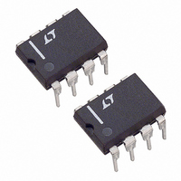
LTC1291DCN8#PBF Linear Technology, LTC1291DCN8#PBF Datasheet - Page 2

LTC1291DCN8#PBF
Manufacturer Part Number
LTC1291DCN8#PBF
Description
IC DATA ACQ SYSTEM 12BIT 8-DIP
Manufacturer
Linear Technology
Type
Data Acquisition System (DAS)r
Datasheet
1.LTC1291DCN8PBF.pdf
(20 pages)
Specifications of LTC1291DCN8#PBF
Resolution (bits)
12 b
Data Interface
Serial, Parallel
Voltage Supply Source
Single Supply
Voltage - Supply
5V
Operating Temperature
0°C ~ 70°C
Mounting Type
Through Hole
Package / Case
8-DIP (0.300", 7.62mm)
Number Of Elements
1
Resolution
12Bit
Architecture
SAR
Sample Rate
54KSPS
Input Polarity
Unipolar
Input Type
Voltage
Rated Input Volt
5V
Differential Input
Yes
Power Supply Requirement
Single
Single Supply Voltage (typ)
5V
Dual Supply Voltage (typ)
Not RequiredV
Dual Supply Voltage (min)
Not RequiredV
Dual Supply Voltage (max)
Not RequiredV
Power Dissipation
500mW
Differential Linearity Error
±1LSB(Typ)
Integral Nonlinearity Error
±0.75LSB
Operating Temp Range
0C to 70C
Operating Temperature Classification
Commercial
Mounting
Through Hole
Pin Count
8
Package Type
PDIP N
Lead Free Status / RoHS Status
Lead free / RoHS Compliant
Sampling Rate (per Second)
-
Lead Free Status / Rohs Status
Compliant
Available stocks
Company
Part Number
Manufacturer
Quantity
Price
LTC1291
A
(Notes 1 and 2)
CO VERTER A D
otherwise specifications are at T
Supply Voltage (V
Voltage
Power Dissipation ............................................. 500mW
Operating Temperature Range
Storage Temperature Range ................. –65 C to 150 C
Lead Temperature (Soldering, 10 sec)................. 300 C
AC CHARACTERISTICS
SYMBOL
f
t
t
t
t
PARAMETER
Offset Error
Linearity Error (INL)
Gain Error
Minimum Resolution for which No
Missing Codes are Guaranteed
Analog Input Range
On Channel Leakage Current
Off Channel Lekage Current
2
which apply over the full operating temperature range, otherwise specifications are at T
CLK
SMPL
CONV
CYC
dDO
(Note 8)
(Note 8)
BSOLUTE
Analog Inputs ............................ –0.3V to V
Digital Inputs ........................................ –0.3V to 12V
Digital Outputs .......................... –0.3V to V
LTC1291BC, LTC1291CC,
LTC1291DC ............................................ 0 C to 70 C
U
PARAMETER
Clock Frequency
Analog Input Sample Time
Conversion Time
Total Cycle Time
Delay Time, CLK to D
CC
W
) to GND .................................. 12V
A
U W
XI
W
OUT
A
= 25 C. (Note 3)
Data Valid
U
CONDITIONS
(Note 4)
(Note 4 & 5)
(Note 4)
(Note 7)
On Channel = 5V
Off Channel = 0V
On Channel = 0V
Off Channel = 5V
On Channel = 5V
Off Channel = 0V
On Channel = 0V
Off Channel = 5V
W
ULTIPLEXER CHARACTERISTICS
The
R
A
denotes the specifications which apply over the full operating temperature range,
TI
CONDITIONS
V
See Operating Sequence
See Operating Sequence
See Operating Sequence (Note 6)
See Test Circuits
CC
U
= 5V (Note 6)
CC
CC
G
+ 0.3V
+ 0.3V
S
MIN
LTC1291B
PACKAGE/ORDER I FOR ATIO
Consult LTC Marketing for parts specified with wider operating temperature ranges.
TYP MAX
GND
CH0
CH1
CS
T
T
JMAX
JMAX
12
1
3
4
2
3.0
0.5
1.0
8-LEAD CERAMIC DIP
8-LEAD PLASTIC DIP
1
1
1
1
= 100 C,
= 150 C,
N8 PACKAGE
J8 PACKAGE
TOP VIEW
– 0.05V to V
MIN
Consider N8 Package for Alternate Source
OBSOLETE PACKAGE
A
JA
JA
LTC1291C
= 25 C. (Note 3)
= 130 C/ W (N8)
= 100 C/ W (J8)
LTC1291B/LTC1291C/LTC1291D
TYP MAX
8
7
6
5
CC
(Note 9)
+ 500ns
18 CLK
MIN
V
CLK
D
D
+ 0.05V
CC
IN
OUT
The
12
3.0
0.5
2.0
1
1
1
1
(V
REF
)
TYP
160
2.5
12
denotes the specifications
U
MIN
LTC1291D
MAX
LTC1291BCN8
LTC1291CCN8
LTC1291DCN8
LTC1291BCJ8
LTC1291CCJ8
LTC1291DCJ8
TYP MAX
300
1.0
ORDER PART
NUMBER
W
0.75
12
3.0
4.0
1
1
1
1
CLK Cycles
CLK Cycles
UNITS
Cycles
UNITS
1291fa
U
MHz
LSB
LSB
LSB
Bits
ns
V
A
A
A
A


