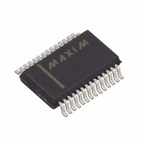
MAX1271BEAI+ Maxim Integrated Products, MAX1271BEAI+ Datasheet - Page 10

MAX1271BEAI+
Manufacturer Part Number
MAX1271BEAI+
Description
IC ADC 12BIT 8CH 28-SSOP
Manufacturer
Maxim Integrated Products
Type
Data Acquisition System (DAS)r
Datasheet
1.MAX1270BCAI.pdf
(20 pages)
Specifications of MAX1271BEAI+
Resolution (bits)
12 b
Sampling Rate (per Second)
110k
Data Interface
Serial
Voltage Supply Source
Single Supply
Voltage - Supply
4.75 V ~ 5.25 V
Operating Temperature
-40°C ~ 85°C
Mounting Type
Surface Mount
Package / Case
28-SSOP
Number Of Adc Inputs
8
Architecture
SAR
Conversion Rate
110 KSPs
Resolution
12 bit
Interface Type
Serial
Voltage Reference
Internal 4.096 V or External
Supply Voltage (max)
5 V
Mounting Style
SMD/SMT
Lead Free Status / RoHS Status
Lead free / RoHS Compliant
Multirange, +5V, 8-Channel,
Serial 12-Bit ADCs
The ADC’s input small-signal bandwidth depends on the
selected input range and varies from 1.5MHz to 5MHz
(see Electrical Characteristics). The MAX1270B/
MAX1271B maximum sampling rate is 110ksps (100ksps
for the MAX1270A/MAX1271A). By using undersampling
techniques, it is possible to digitize high-speed transient
events and measure periodic signals with bandwidths
exceeding the ADC’s sampling rate.
To avoid high-frequency signals being aliased into the
frequency band of interest, anti-aliasing filtering is rec-
ommended.
The MAX1270/MAX1271 have software-selectable input
ranges. Each analog input channel can be indepen-
dently programmed to one of four ranges by setting the
appropriate control bits (RNG, BIP) in the control byte
(Table 1). The MAX1270 has selectable input ranges
extending to ±10V (±V
has selectable input ranges extending to ±V
4 shows the equivalent input circuit.
A resistor network on each analog input provides
±16.5V fault protection for all channels. Whether or not
the channel is on, this circuit limits the current going
into or out of the pin to less than 2mA. This provides an
added layer of protection when momentary overvolt-
ages occur at the selected input channel, when a neg-
ative signal is applied to the input, and when the device
is configured for unipolar mode. The overvoltage pro-
tection is active even if the device is in power-down
mode or if V
Figure 5. Detailed Serial-Interface Timing
10
______________________________________________________________________________________
DOUT
SCLK
DIN
CS
DD
= 0.
t
CSH
Input Range and Protection
REF
t
DV
t
x 2.441), while the MAX1271
CSS
t
DS
t
DH
Input Bandwidth
t
CL
REF
. Figure
t
CH
The MAX1270/MAX1271 feature a serial interface that is
fully compatible with SPI/QSPI and MICROWIRE devices.
For SPI/QSPI, set CPOL = 0, CPHA = 0 in the SPI control
registers of the microcontroller. Figure 5 shows detailed
serial-interface timing information. See Table 1 for details
on programming the input control byte.
Figure 4. Equivalent Input Circuit
CH_
S1 = BIPOLAR/UNIPOLAR SWITCH
S2 = INPUT MUX SWITCH
S3, S4 = T/H SWITCH
R1
R3
5.12kΩ
t
DO
S1
S2
R2
HOLD
UNIPOLAR
OFF
ON
BIPOLAR
t
CSH
S3
R1 = 12.5kΩ (MAX1270)
R2 = 8.67kΩ (MAX1270)
TRACK
or 5.12kΩ (MAX1271)
Digital Interface
t
C
TR
HOLD
or ∞ (MAX1271)
TRACK
S4
VOLTAGE
REFERENCE
T/H
OUT
HOLD


