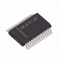
MAX1271BEAI+ Maxim Integrated Products, MAX1271BEAI+ Datasheet - Page 14

MAX1271BEAI+
Manufacturer Part Number
MAX1271BEAI+
Description
IC ADC 12BIT 8CH 28-SSOP
Manufacturer
Maxim Integrated Products
Type
Data Acquisition System (DAS)r
Datasheet
1.MAX1270BCAI.pdf
(20 pages)
Specifications of MAX1271BEAI+
Resolution (bits)
12 b
Sampling Rate (per Second)
110k
Data Interface
Serial
Voltage Supply Source
Single Supply
Voltage - Supply
4.75 V ~ 5.25 V
Operating Temperature
-40°C ~ 85°C
Mounting Type
Surface Mount
Package / Case
28-SSOP
Number Of Adc Inputs
8
Architecture
SAR
Conversion Rate
110 KSPs
Resolution
12 bit
Interface Type
Serial
Voltage Reference
Internal 4.096 V or External
Supply Voltage (max)
5 V
Mounting Style
SMD/SMT
Lead Free Status / RoHS Status
Lead free / RoHS Compliant
Multirange, +5V, 8-Channel,
Serial 12-Bit ADCs
Figure 9. Internal Clock Mode—20 SCLK/Conversion Timing
Figure 10. Internal Clock Mode—SSTRB Detailed Timing
conversion in progress. Figure 10 shows the SSTRB
timing in internal clock mode.
Internal clock mode conversions can be completed
with 13 external clocks per conversion but require a
waiting period of 15µs for the conversion to be com-
pleted (Figure 11).
Most microcontrollers require that conversions occur in
multiples of 8 SCLK clock cycles. Sixteen clock cycles
per conversion (as shown in Figure 12) is typically the
most convenient way for a microcontroller to drive the
MAX1270/MAX1271.
14
SSTRB
______________________________________________________________________________________
SCLK
CS
SSTRB
DOUT
A/D STATE
SCLK
DIN
CS
HIGH-Z
START SEL2 SEL1 SEL0 RNG
MSB
1
SCLK #8
t
CSH
BIP
PD1
ACQUISITION
2 EXT SCLK
+4 INT CLK
PD0
LSB
t
SSTRB
8
16 INT CLK
CONVERSION
12 INT CLK
HIGH-Z
NOTE: FOR BEST NOISE PERFORMANCE, KEEP SCLK LOW DURING CONVERSION.
The MAX1270/MAX1271 power up in normal operation
(all internal circuitry active) and internal clock mode,
waiting for a start bit. The contents of the output data
register are cleared at power-up.
The MAX1270/MAX1271 operate with either an internal
or external reference. An external reference is connect-
ed to either REF or REFADJ (Figure 13). The REFADJ
internal buffer gain is trimmed to 1.638V to provide
4.096V at REF from a 2.5V reference.
MSB
D11 D10
9
10
D1
19
LSB
D0
20
Applications Information
Internal or External Reference
t
FILLED WITH ZEROS
SCK
Power-On Reset
t
CSS
HIGH-Z


