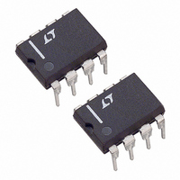
LTC1287CCN8 Linear Technology, LTC1287CCN8 Datasheet - Page 7

LTC1287CCN8
Manufacturer Part Number
LTC1287CCN8
Description
IC DATA ACQ SYS 12BIT 3V 8-DIP
Manufacturer
Linear Technology
Type
Data Acquisition System (DAS)r
Datasheet
1.LTC1287CCN8.pdf
(16 pages)
Specifications of LTC1287CCN8
Resolution (bits)
12 b
Sampling Rate (per Second)
30k
Data Interface
Serial, Parallel
Voltage Supply Source
Single Supply
Voltage - Supply
3V
Operating Temperature
0°C ~ 70°C
Mounting Type
Through Hole
Package / Case
8-DIP (0.300", 7.62mm)
Lead Free Status / RoHS Status
Contains lead / RoHS non-compliant
Available stocks
Company
Part Number
Manufacturer
Quantity
Price
Company:
Part Number:
LTC1287CCN8
Manufacturer:
TI
Quantity:
190
The LTC1287 is a data acquisition component which
contains the following functional blocks:
1. 12-bit successive approximation capacitive A/D
2. Analog multiplexer (MUX)
3. Sample-and-hold (S/H)
4. Synchronous, half-duplex serial interface
5. Control and timing logic
DIGITAL CONSIDERATIONS
Serial Interface
The LTC1287 communicates with microprocessors and
other external circuitry via a synchronous, half-duplex,
three-wire serial interface (see Operating Sequence). The
clock (CLK) synchronizes the data transfer with each bit
being transmitted on the falling CLK edge. The LTC1287
A
TEST CIRCUITS
D
PPLICATI
CLK
converter
OUT
CS
t
SMPL
Hi-Z
D
CLK
OUT
CS
O
B11
U
B10
S
B9
I FOR ATIO
U
B8
B7
t
CONV
W
B6
B5
Figure 1. LTC1287 Operating Sequence
B4
Voltage Waveforms for t
B3
U
B2
B1
t
CYC
B0
t
en
does not require a configuration input word and has no D
pin. It is permanently configured to have a single differen-
tial input and to operate in unipolar mode. A falling CS
initiates data transfer. The first CLK pulse enables D
After one null bit, the A/D conversion result is output on the
D
first sequence. With the half duplex serial interface the
D
easy interface to MSB- or LSB-first serial ports. Bringing
CS high resets the LTC1287 for the next data exchange.
Logic Levels
The logic level standards for this supply range have not
been well defined. What standards that do exist are not
universally accepted. The trip point on the logic inputs of
the LTC1287 is 0.28
compatible with HC-type levels and processors that are
OUT
OUT
B1
0.6V
B2
line with a MSB-first sequence followed by a LSB-
data is from the current conversion. This provides
en
B3
B4
B5
B6
V
B7
CC
B8
. This makes the logic inputs
B11
B9
LTC1287 TC07
B10
B11
LTC1287
LTC1287 F01
t
SMPL
OUT
1287fa
7
IN
.


