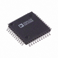
AD2S1200YSTZ Analog Devices Inc, AD2S1200YSTZ Datasheet - Page 17

AD2S1200YSTZ
Manufacturer Part Number
AD2S1200YSTZ
Description
IC CONV R/D 12-BIT W/OSC 44-LQFP
Manufacturer
Analog Devices Inc
Type
R/D Converterr
Datasheet
1.AD2S1200.pdf
(24 pages)
Specifications of AD2S1200YSTZ
Resolution (bits)
12 b
Data Interface
Serial, Parallel
Voltage Supply Source
Analog and Digital
Voltage - Supply
4.75 V ~ 5.25 V
Operating Temperature
-40°C ~ 125°C
Mounting Type
Surface Mount
Package / Case
44-LQFP
Input Channel Type
Differential
Supply Voltage Range - Analog
4.75V To 5.25V
Supply Voltage Range - Digital
4.75V To 5.25V
Lead Free Status / RoHS Status
Lead free / RoHS Compliant
For Use With
EVAL-AD2S1200CBZ - BOARD EVAL FOR AD2S1200
Sampling Rate (per Second)
-
Lead Free Status / RoHS Status
Lead free / RoHS Compliant, Lead free / RoHS Compliant
Available stocks
Company
Part Number
Manufacturer
Quantity
Price
Company:
Part Number:
AD2S1200YSTZ
Manufacturer:
Analog Devices Inc
Quantity:
10 000
Synthetic Reference Generation
When a resolver undergoes a high rotation rate, the RDC tends
to act as an electric motor and produces speed voltages, along
with the ideal Sin and Cos outputs. These speed voltages are in
quadrature to the main signal waveform. Moreover, nonzero
resistance in the resolver windings causes a non-zero phase shift
between the reference input and the Sin and Cos outputs. The
combination of speed voltages and phase shift causes a tracking
error in the RDC that is approximated by
To compensate for the described phase error between the
resolver reference excitation and the Sin/Cos signals, an internal
synthetic reference signal is generated in phase with the refer-
ence frequency carrier. The synthetic reference is derived using
the internally filtered Sin and Cos signals. It is generated by
determining the zero crossing of either the Sin or Cos (which-
ever signal is larger, to improve phase accuracy) and evaluating
the phase of the resolver reference excitation. The synthetic
reference reduces the phase shift between the reference and
Sin/Cos inputs to less than 10°, and will operate for phase shifts
of ±45°.
SUPPLY SEQUENCING AND RESET
The AD2S1200 requires an external reset signal to hold the
RESET input low until V
range of 4.5 V to 5.5 V.
The RESET pin must be held low for a minimum of 10 µs after
V
RESET signal to the AD2S1200 initializes the output position to
a value of 0x000 (degrees output through the parallel, serial, and
encoder interfaces) and causes LOS to be indicated (LOT and
DOS pins pulled low) as shown in Figure 10.
Failure to apply the above (correct) power-up/reset sequence
can result in an incorrect position indication.
DD
is within the specified range (t
Error
=
Phase
DD
Shift
is within the specified operating
×
Reference
RST
Rotation
in Figure 10). Applying a
Frequency
Rate
Rev. 0 | Page 17 of 24
After a rising edge on the RESET input, the device must be
allowed at least 20 ms (t
circuitry to stabilize and the tracking loop to settle to the step
change in input position. After t
applied, releasing the LOT and DOT pins to the state deter-
mined by the fault detection circuitry and providing valid
position data at the parallel and serial outputs (note that if
position data is being acquired via the encoder outputs, they
may be monitored during t
The RESET pin is internally pulled up.
CHARGE PUMP OUTPUT
A 204.8 kHz square wave output with 50% duty cycle is avail-
able at the CPO output pin of the AD2S1200. This square wave
output can be used for negative rail voltage generation, or to
create a V
SAMPLE
RESET
DOS
LOT
V
DD
CC
4.75V
rail.
Figure 10. Power Supply Sequencing and Reset
t
t
RST
RST
TRACK
TRACK
) as shown in Figure 10 for internal
t
TRACK
).
TRACK
, a SAMPLE pulse must be
AD2S1200
VALID
OUTPUT
DATA


