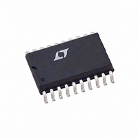
LTC1289CCSW#TR Linear Technology, LTC1289CCSW#TR Datasheet - Page 12

LTC1289CCSW#TR
Manufacturer Part Number
LTC1289CCSW#TR
Description
IC DATA ACQ SYS 12BIT 3V 20SOIC
Manufacturer
Linear Technology
Type
Data Acquisition System (DAS)r
Datasheet
1.LTC1289CCN.pdf
(28 pages)
Specifications of LTC1289CCSW#TR
Resolution (bits)
12 b
Sampling Rate (per Second)
25k
Data Interface
Serial, Parallel
Voltage Supply Source
Dual ±
Voltage - Supply
3V
Operating Temperature
0°C ~ 70°C
Mounting Type
Surface Mount
Package / Case
20-SOIC (7.5mm Width)
Lead Free Status / RoHS Status
Contains lead / RoHS non-compliant
Available stocks
Company
Part Number
Manufacturer
Quantity
Price
INPUT
CONFIGURATION
Single-Ended
Differential
The reference voltages REF
V
than or equal to V
or equal to V
The following examples are for a single-ended input con-
figuration.
Example 1: Let V
and COM = 0V. Unipolar mode of operation. The resulting
input span is 0V ≤ IN
Example 2: The same conditions as Example 1 except
COM = 1V. The resulting input span is 1V ≤ IN
if IN
the resulting D
Example 3: Let V
= 1V and COM = 1V. Bipolar mode of operation. The
resulting input span is –1V ≤ IN+ ≤ 3V.
For differential input configurations with the same condi-
tions as in the above three examples the resulting input
spans are as follows:
Example 1 (Diff.): IN
LTC1289
The following discussion will demonstrate how the two
reference pins are to be used in conjunction with the
analog input multiplexer. In unipolar mode the input span
of the A/D is set by the difference in voltage on the REF
and the REF
twice the difference in voltage on the REF
REF
span is set by the voltage on the COM pin for single-ended
inputs and by the voltage on the minus input pin for
differential inputs. For the bipolar mode of operation the
voltage on the COM pin or the minus input pin sets the
center of the input span.
The upper and lower value of the input span can now be
summarized in the following table:
12
A
CC
PPLICATI
+
–
and V
≥ 3V the resulting D
pin. In the unipolar mode the lower value of the input
–
, but the difference (REF
Lower Value COM
Upper Value (REF
Lower Value IN
Upper Value (REF
–
CC
pin. In the bipolar mode the input span is
OUT
and greater than or equal to V
CC
O
CC
CC
word is all 0’s.
. The input voltages must be less than
= 3.3V, V
= 3.3V, V
U
+
–
UNIPOLAR MODE
S
≤ 2V.
≤
–
OUT
IN
+
+
I FOR ATIO
– REF
– REF
U
+
+
word is all 1’s. If IN
–
–
≤
and REF
= 0V, REF
= –3.3V, REF
IN
–
–
) + COM (REF
) + IN
–
+
+ 2V
– REF
–
W
–
+
BIPOLAR MODE
–(REF
–(REF
(REF
can fall between
= 3V, REF
–
) must be less
+
+
+
+
+
+
– REF
– REF
+
pin and the
– REF
– REF
= 3V, REF
–
+
≤ 3V. Note
.
≤ 1V then
U
–
–
) + COM
–
–
) + IN
) + COM
) + IN
–
+
= 1V
pin
–
–
–
Example 2 (Diff.): IN
Example 3 (Diff.): IN
MSB-First/LSB-First Format (MSBF)
The output data of the LTC1289 is programmed for MSB-
first or LSB-first sequence using the MSBF bit. For MSB-
first output data, the input word clocked to the LTC1289
should always contain a logical one in the sixth bit location
(MSBF bit). Likewise for LSB-first output data the input
word clocked to the LTC1289 should always contain a zero
in the MSBF bit location. The MSBF bit affects only the
order of the output data word. The order of the input word
is unaffected by this bit.
Word Length (WL1, WL0) and Power Shutdown
The last two bits of the input word (WL1 and WL0)
program the output data word length and the power
shutdown feature of the LTC1289. Word lengths of 8, 12
or 16 bits can be selected according to the following table.
The WL1 and WL0 bits in a given D
length of the present, not the next, D
WL0 are never “don’t cares” and must be set for the
correct D
is sent. On any transfer cycle, the word length should be
made equal to the number of SCLK cycles sent by the
MPU. Power down will occur when WL1 = 0 and WL0 = 1
is selected. The previous result will be clocked out as a 10
bit word so a “dummy”conversion is required before
powering down the LTC1289. Conversions are resumed
once CS goes low or an SCLK is applied, if CS is already
low.
WL1
0
0
1
1
MSBF
OUT
0
1
word length even when a “dummy” D
WL0
0
1
0
1
–
–
– 2V
≤
IN
+
≤
≤
OUTPUT WORD LENGTH
IN
IN
OUTPUT FORMAT
+
–
Power Shutdown
≤
+ 2V
MSB-First
LSB-First
IN
IN
OUT
12 Bits
16 Bits
8 Bits
–
word control the
+ 2V.
word. WL1 and
IN
word
LTC1289 AI06
LTC1289 AI07
1289fb


