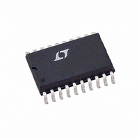
LTC1289CCSW#TR Linear Technology, LTC1289CCSW#TR Datasheet - Page 3

LTC1289CCSW#TR
Manufacturer Part Number
LTC1289CCSW#TR
Description
IC DATA ACQ SYS 12BIT 3V 20SOIC
Manufacturer
Linear Technology
Type
Data Acquisition System (DAS)r
Datasheet
1.LTC1289CCN.pdf
(28 pages)
Specifications of LTC1289CCSW#TR
Resolution (bits)
12 b
Sampling Rate (per Second)
25k
Data Interface
Serial, Parallel
Voltage Supply Source
Dual ±
Voltage - Supply
3V
Operating Temperature
0°C ~ 70°C
Mounting Type
Surface Mount
Package / Case
20-SOIC (7.5mm Width)
Lead Free Status / RoHS Status
Contains lead / RoHS non-compliant
Available stocks
Company
Part Number
Manufacturer
Quantity
Price
CO VERTER A D
AC CHARACTERISTICS
which apply over the full operating temperature range, otherwise specifications are at T
PARAMETER
Minimum Resolution for
Which No Missing Codes are
Guaranteed
Analog and REF Input Range
On Channel Leakage Current
(Note 8)
Off Channel Leakage Current
(Note 8)
otherwise specifications are at T
SYMBOL
f
f
t
t
t
t
t
t
t
t
t
t
t
t
t
t
t
C
SCLK
ACLK
ACC
SMPL
CONV
CYC
dDO
dis
en
hCS
hDI
hDO
f
r
suDI
suCS
WHCS
IN
U
PARAMETER
Shift Clock Frequency
A/D Clock Frequency
Delay time from CS↓ to D
Analog Input Sample Time
Conversion Time
Total Cycle Time
Delay Time, SCLK↓ to D
Delay Time, CS↑ to D
Delay Time, 2nd ACLK↓ to D
Hold Time, CS After Last SCLK↓
Hold Time, D
Time Output Data Remains Valid After SCLK↓
D
D
Setup Time, D
Setup Time, CS↓ Before Clocking in
First Address Bit
CS High Time During Conversion
Input Capacitance
OUT
OUT
Fall Time
Rise Time
IN
IN
After SCLK↑
Stable Before SCLK↑
U W
OUT
CONDITIONS
(Note 7)
On Channel = 3V
Off Channel = 0V
On Channel = 0V
Off Channel = 3V
On Channel = 3V
Off Channel = 0V
On Channel = 0V
Off Channel = 3V
A
OUT
OUT
Hi-Z
= 25°C. (Note 3)
Data Valid
OUT
Data Valid
ULTIPLEXER CHARACTERISTICS
Enabled
The
●
denotes the specifications which apply over the full operating temperature range,
●
●
●
●
●
MIN
CONDITIONS
(Note 6)
(Note 6)
(Note 9)
See Operating Sequence
See Operating Sequence
See Operating Sequence (Note 6)
See Test Circuits
See Test Circuits
See Test Circuits
(Note 6)
(Note 6)
See Test Circuits
See Test Circuits
(Note 6 and 9)
(Note 6 and 9)
(Note 6)
Analog Inputs On Channel
Analog Inputs Off Channel
Digital Inputs
(V
–
) – 0.05V to V
LTC1289B
TYP
CC
+ 0.05V
MAX
12
±1
±1
±1
±1
A
= 25°C. (Note 3)
●
●
●
●
●
MIN
(V
–
(Note 10)
) – 0.05V to V
12 SCLK +
56 ACLK
2 ACLK Cycles
+ 180ns
The
MIN
50
50
52
0
0
LTC1289C
●
denotes the specifications
LTC1289B
LTC1289C
TYP
TYP
200
130
100
52
70
50
40
40
2
7
5
5
CC
+ 0.05V
MAX
350
150
250
100
100
1.0
2.0
LTC1289
MAX
12
±1
±1
±1
±1
UNITS
UNITS
Cycles
Cycles
Cycles
Cycles
Cycles
ACLK
SCLK
ACLK
ACLK
1289fb
3
BITS
MHz
MHz
µA
µA
µA
µA
ns
ns
ns
ns
ns
ns
ns
ns
ns
pF
pF
pF
V


