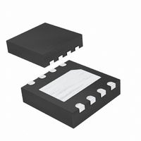
MAX5423ETA+T Maxim Integrated Products, MAX5423ETA+T Datasheet - Page 4

MAX5423ETA+T
Manufacturer Part Number
MAX5423ETA+T
Description
IC POT DGTL 256-TAP NV 8-TDFN
Manufacturer
Maxim Integrated Products
Datasheet
1.MAX5423ETAT.pdf
(11 pages)
Specifications of MAX5423ETA+T
Taps
256
Resistance (ohms)
100K
Number Of Circuits
1
Temperature Coefficient
35 ppm/°C Typical
Memory Type
Non-Volatile
Interface
SPI, 3-Wire Serial
Voltage - Supply
2.7 V ~ 5.25 V
Operating Temperature
-40°C ~ 85°C
Mounting Type
Surface Mount
Package / Case
8-TDFN Exposed Pad
Resistance In Ohms
100K
Number Of Pots
Single
Taps Per Pot
256
Resistance
100 KOhms
Wiper Memory
Non Volatile
Digital Interface
Serial (3-Wire, SPI)
Operating Supply Voltage
5 V
Supply Current
0.001 mA
Maximum Operating Temperature
+ 85 C
Minimum Operating Temperature
- 40 C
Description/function
100kOhm, 256-Tap, Nonvolatile, SPI-Interface Digital Potentiometer
Mounting Style
SMD/SMT
Supply Voltage (max)
5.25 V
Supply Voltage (min)
2.7 V
Tolerance
25 %
Lead Free Status / RoHS Status
Lead free / RoHS Compliant
Other names
MAX5423ETA+T
MAX5423ETA+TTR
MAX5423ETA+TTR
256-Tap, Nonvolatile, SPI-Interface,
Digital Potentiometers
TIMING CHARACTERISTICS (continued)
(V
noted. See Figure 1.) (Note 7)
Note 1: The DNL and INL are measured with the potentiometer configured as a voltage-divider with H = V
Note 2: The DNL and INL are measured with the potentiometer configured as a variable resistor. H is unconnected and L = GND.
Note 3: The wiper resistance is measured using the source currents given in Note 2. For operation to V
Note 4: The device draws higher supply current when the digital inputs are driven with voltages between (V
Note 5: Wiper at midscale with a 10pF load (DC measurement). L = GND; an AC source is applied to H; and the W output is mea-
Note 6: The programming current operates only during power-up and NV writes.
Note 7: Digital timing is guaranteed by design and characterization, and is not production tested.
Note 8: Wiper-settling time is the worst-case 0% to 50% rise-time measured between consecutive wiper positions. H = V
4
(V
DIN Hold after SCLK
SCLK Rise to CS Fall Delay
CS Rise to SCLK Rise Hold
CS Pulse-Width High
Write NV Register Busy Time
DD
-0.05
-0.10
-0.15
-0.20
-0.25
DD
0.25
0.20
0.15
0.10
0.05
_______________________________________________________________________________________
0
= +2.7V to +5.25V, H = V
= 5.0V, T
0
wiper terminal is unloaded and measured with a high-input-impedance voltmeter.
For the 5V condition, the wiper terminal is driven with a source current of 80µA for the 50kΩ configuration, 40µA for the
100kΩ configuration, and 20µA for the 200kΩ configuration. For the 3V condition, the wiper terminal is driven with a source
current of 40µA for the 50kΩ configuration, 20µA for the 100kΩ, and 10µA for the 200kΩ configuration.
Wiper Resistance vs. Temperature in the Typical Operating Characteristics.
0.5V). See Supply Current vs. Digital Input Voltage in the Typical Operating Characteristics.
sured. A 3dB bandwidth occurs when the AC W/H value is 3dB lower than the DC W/H value.
GND, and the wiper terminal is unloaded and measured with a 10pF oscilloscope probe.
VOLTAGE-DIVIDER MODE
PARAMETER
32
DNL vs. TAP POSITION
64
A
= +25°C, unless otherwise noted.)
96
TAP POSITION
128 160
192
DD
, L = GND, T
224
SYMBOL
256
t
t
t
t
BUSY
CSW
t
CS0
CS1
DH
A
-0.05
-0.10
-0.15
-0.20
-0.25
0.25
0.20
0.15
0.10
0.05
= -40°C to +85°C. Typical values are at V
0
0
VOLTAGE-DIVIDER MODE
32
INL vs. TAP POSITION
64
96
TAP POSITION
CONDITIONS
128 160
Typical Operating Characteristics
192
224
256
DD
700
600
500
400
300
200
100
= +5.0V, T
0
MIN
200
0
20
80
WIPER RESISTANCE vs. TAP POSITION
0
V
I
SRC
DD
32
DD
= 2.7V
= 50μA
A
DD
64
= 2.7V, see Maximum
= +25°C, unless otherwise
TYP
DD
and L = GND. The
96
TAP POSITION
- 0.5V) and (GND +
128 160
MAX
12
DD
192
, L =
UNITS
ms
ns
ns
ns
ns
224
256


