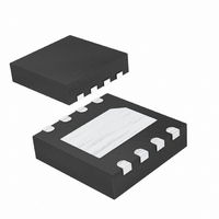
MAX5423ETA+T Maxim Integrated Products, MAX5423ETA+T Datasheet - Page 8

MAX5423ETA+T
Manufacturer Part Number
MAX5423ETA+T
Description
IC POT DGTL 256-TAP NV 8-TDFN
Manufacturer
Maxim Integrated Products
Datasheet
1.MAX5423ETAT.pdf
(11 pages)
Specifications of MAX5423ETA+T
Taps
256
Resistance (ohms)
100K
Number Of Circuits
1
Temperature Coefficient
35 ppm/°C Typical
Memory Type
Non-Volatile
Interface
SPI, 3-Wire Serial
Voltage - Supply
2.7 V ~ 5.25 V
Operating Temperature
-40°C ~ 85°C
Mounting Type
Surface Mount
Package / Case
8-TDFN Exposed Pad
Resistance In Ohms
100K
Number Of Pots
Single
Taps Per Pot
256
Resistance
100 KOhms
Wiper Memory
Non Volatile
Digital Interface
Serial (3-Wire, SPI)
Operating Supply Voltage
5 V
Supply Current
0.001 mA
Maximum Operating Temperature
+ 85 C
Minimum Operating Temperature
- 40 C
Description/function
100kOhm, 256-Tap, Nonvolatile, SPI-Interface Digital Potentiometer
Mounting Style
SMD/SMT
Supply Voltage (max)
5.25 V
Supply Voltage (min)
2.7 V
Tolerance
25 %
Lead Free Status / RoHS Status
Lead free / RoHS Compliant
Other names
MAX5423ETA+T
MAX5423ETA+TTR
MAX5423ETA+TTR
(CS), data clock (SCLK), and data in (DIN). Drive CS
low to enable the serial interface and clock data syn-
chronously into the shift register on each SCLK rising
edge.
The WRITE commands (C1, C0 = 00 or 01) require 16
clock cycles to clock in the command and data (Figure
2a). The COPY commands (C1, C0 = 10, 11) can use
either eight clock cycles to transfer the command bits
(Figure 2b) or 16 clock cycles with 8 data bits that are
disregarded by the device (Figure 2a).
256-Tap, Nonvolatile, SPI-Interface,
Digital Potentiometers
Table 1. Register Map
Figure 2. Digital-Interface Format
8
Bit name
Write wiper register
Write NV register
Copy wiper register to NV
register
Copy NV register to wiper
register
_______________________________________________________________________________________
CLOCK EDGE
A) 16-BIT COMMAND/DATA WORD
B) 8-BIT COMMAND WORD
SCLK
SCLK
DIN
DIN
CS
CS
1
1
—
1
0
0
0
0
2
2
—
2
0
0
0
0
C1
C1
3
3
C1
3
0
0
1
1
C0
C0
4
4
C0
4
0
1
0
1
5
5
—
5
0
0
0
0
6
6
—
7
7
6
0
0
0
0
8
8
After loading data into the shift register, drive CS high
to latch the data into the appropriate potentiometer
control register and disable the serial interface. Keep
CS low during the entire serial-data stream to avoid
corruption of the data.
The serial-data timing for the potentiometer is shown in
Figures 1 and 2.
—
7
0
0
0
0
D7
9
—
8
0
0
0
0
D6
10
D7
D7
D7
—
—
9
11
D5
10
D6
D6
D6
—
—
D4
12
D5
D5
D5
11
—
—
13
D3
D4
D4
D4
12
—
—
D2
14
15
D1
D3
D3
D3
13
—
—
D0
16
D2
D2
D2
14
—
—
D1
D1
D1
15
—
—
D0
D0
D0
16
—
—


