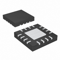
MAX5496ETE+ Maxim Integrated Products, MAX5496ETE+ Datasheet - Page 13

MAX5496ETE+
Manufacturer Part Number
MAX5496ETE+
Description
IC DGTL POT 10BIT 16-TQFN-EP
Manufacturer
Maxim Integrated Products
Datasheet
1.MAX5494ETE.pdf
(20 pages)
Specifications of MAX5496ETE+
Taps
1024
Resistance (ohms)
10K
Number Of Circuits
2
Temperature Coefficient
35 ppm/°C Typical
Memory Type
Non-Volatile
Interface
3-Wire Serial
Voltage - Supply
2.5 V ~ 5.25 V
Operating Temperature
-40°C ~ 85°C
Mounting Type
Surface Mount
Package / Case
16-TQFN Exposed Pad
Resistance In Ohms
10K
Number Of Pots
Dual
Taps Per Pot
1024
Resistance
10 KOhms
Wiper Memory
Non Volatile
Digital Interface
Serial (3-Wire, SPI)
Operating Supply Voltage
2.7 V to 5.25 V
Supply Current
1.5 uA
Maximum Operating Temperature
+ 85 C
Minimum Operating Temperature
- 40 C
Description/function
1024-Tap Dual 10k Nonvolatile Linear-Taper Digital Potentiometer (Variable Resistor)
Mounting Style
SMD/SMT
Supply Voltage (max)
5.25 V
Supply Voltage (min)
2.7 V
Tolerance
25 %
Lead Free Status / RoHS Status
Lead free / RoHS Compliant
resistance is equal to the nominal end-to-end resis-
tance divided by 1024 (10-bit resolution). For example,
the programmable resolution is 9.8Ω and 48.8Ω for the
MAX5496/MAX5498 and the MAX5497/MAX5499,
respectively.
The 10-bit data in the 10-bit latch register selects the
wiper position from the 1024 possible positions, result-
ing in 1024 values for the resistance from W_ to L_.
Calculate the resistance from W_ to L_ (R
formula below:
where D is decimal equivalent of the 10 data bits writ-
ten, R
is the zero-scale error. Table 1 shows R
codes.
The MAX5494–MAX5499 use a 3-wire, SPI-compatible,
serial data interface (Figure 6). This write-only interface
contains three inputs: chip-select (CS), data input
(DIN), and data clock (SCLK). Drive CS low to enable
the serial interface and clock data synchronously into
the shift register on each SCLK rising edge.
The WRITE commands (C1, C0 = 00 or 01) require 24
clock cycles to transfer the command and data (Figure
7a). The COPY commands (C1, C0 = 10 or 11) use
Figure 6. SPI-Interface Timing Diagram
W-L
is the nominal end-to-end resistance, and R
SCLK
DIN
CS
R
SPI-Compatible Serial Interface
WL
______________________________________________________________________________________
( )
D
t
CSO
=
10-Bit, Dual, Nonvolatile, Linear-Taper
1023
D
t
×
CSS
R
W L
−
t
DS
+
R
Z
WL
WL
t
at selected
CL
) from the
t
DH
t
CH
Z
either eight clock cycles to transfer the command bits
(Figure 7b) or 24 clock cycles with 16 bits disregarded
by the device (Figure 7a).
After the loading of data into the shift register, drive CS
high to latch the data into the appropriate control regis-
ter (specified by RA1 and RA0) and disable the serial
interface. Keep CS low during the entire serial data
stream to avoid corruption of the data. Table 2 shows
the register map.
The “write wiper register” command (C1, C0 = 00) con-
trols the wiper positions. The 10 data bits (D9–D0) indi-
cate the position of the wiper. For example, if DIN =
000000 0000, the wiper moves to the position closest to
L_. If DIN = 11 1111 1111, the wiper moves closest to H_.
Table 1. R
Digital Potentiometers
CODE (DECIMAL)
1023
512
0
1
t
CP
WL
at Selected Codes
END-TO-END RESISTANCE VALUE
t
CSH
R
10,070
10kΩ
5,070
WL
70
80
(Ω)
t
Write Wiper Register
CS1
t
CSW
R
25,110
50,110
50kΩ
WL
110
160
(Ω)
13


