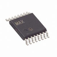
DS1859E-050+ Maxim Integrated Products, DS1859E-050+ Datasheet - Page 27

DS1859E-050+
Manufacturer Part Number
DS1859E-050+
Description
IC RES TEMP 50/50K 3MON 16-TSSOP
Manufacturer
Maxim Integrated Products
Datasheet
1.DS1859E-050.pdf
(28 pages)
Specifications of DS1859E-050+
Taps
256
Resistance (ohms)
50K
Number Of Circuits
2
Temperature Coefficient
50 ppm/°C Typical
Memory Type
Non-Volatile
Interface
I²C, 2-Wire Serial
Voltage - Supply
2.85 V ~ 5.5 V
Operating Temperature
-40°C ~ 95°C
Mounting Type
Surface Mount
Package / Case
16-TSSOP
Resistance In Ohms
50K
Number Of Pots
Dual
Taps Per Pot
256
Resistance
50 KOhms
Wiper Memory
Non Volatile
Digital Interface
Serial (2-Wire)
Operating Supply Voltage
2.85 V to 5.5 V
Supply Current
1 mA
Maximum Operating Temperature
+ 85 C
Minimum Operating Temperature
- 40 C
Mounting Style
SMD/SMT
Supply Voltage (max)
5.5 V
Supply Voltage (min)
2.85 V
Lead Free Status / RoHS Status
Lead free / RoHS Compliant
Accordingly, the following bus conditions have been
defined:
Bus not busy: Both data and clock lines remain high.
Start data transfer: A change in the state of the data
line from high to low while the clock is high defines a
START condition.
Stop data transfer: A change in the state of the data
line from low to high while the clock line is high defines
the STOP condition.
Data valid: The state of the data line represents valid
data when, after a START condition, the data line is sta-
ble for the duration of the high period of the clock signal.
The data on the line can be changed during the low peri-
od of the clock signal. There is one clock pulse per bit of
data. Figures 5 and 6 detail how data transfer is accom-
plished on the 2-wire bus. Depending on the state of the
R/W bit, two types of data transfer are possible.
Each data transfer is initiated with a START condition
and terminated with a STOP condition. The number of
data bytes transferred between START and STOP con-
ditions is not limited and is determined by the master
device. The information is transferred byte-wise and
each receiver acknowledges with a ninth bit.
Within the bus specifications, a standard mode
(100kHz clock rate) and a fast mode (400kHz clock
rate) are defined. The DS1859 works in both modes.
Acknowledge: Each receiving device, when addressed,
is obliged to generate an acknowledge after the byte
has been received. The master device must generate an
extra clock pulse, which is associated with this acknowl-
edge bit.
A device that acknowledges must pull down the SDA line
during the acknowledge clock pulse in such a way that
the SDA line is a stable low during the high period of the
acknowledge-related clock pulse. Setup and hold times
must be taken into account. A master must signal an end
of data to the slave by not generating an acknowledge bit
on the last byte that has been clocked out of the slave. In
this case, the slave must leave the data line high to
enable the master to generate the STOP condition.
1)
2)
the data line while the clock line is high will be
interpreted as control signals.
Data transfer from a master transmitter to a
slave receiver. The first byte transmitted by the
master is the command/control byte. Next follows
a number of data bytes. The slave returns an
acknowledge bit after each received byte.
Data transfer from a slave transmitter to a mas-
ter receiver. The master transmits the first byte
Dual, Temperature-Controlled Resistors with
____________________________________________________________________
Internally Calibrated Monitors
The master device generates all serial clock pulses and
the START and STOP conditions. A transfer is ended with
a STOP condition or with a repeated START condition.
Since a repeated START condition is also the beginning
of the next serial transfer, the bus is not released.
The DS1859 can operate in the following three modes:
1)
2)
3)
(the command/control byte) to the slave. The
slave then returns an acknowledge bit. Next fol-
lows a number of data bytes transmitted by the
slave to the master. The master returns an
acknowledge bit after all received bytes other
than the last byte. At the end of the last received
byte, a not acknowledge can be returned.
Slave Receiver Mode: Serial data and clock are
received through SDA and SCL, respectively. After
each byte is received, an acknowledge bit is trans-
mitted. START and STOP conditions are recog-
nized as the beginning and end of a serial transfer.
Address recognition is performed by hardware
after the slave (device) address and direction bit
have been received.
Slave Transmitter Mode: The first byte is
received and handled as in the slave receiver
mode. However, in this mode the direction bit
indicates that the transfer direction is reversed.
Serial data is transmitted on SDA by the DS1859,
while the serial clock is input on SCL. START and
STOP conditions are recognized as the beginning
and end of a serial transfer.
Slave Address: Command/control byte is the first
byte received following the START condition from
the master device. The command/control byte
consists of 4-bit control code. They are used by
the master device to select which of eight possi-
ble devices on the bus is to be accessed. When
reading or writing to the DS1859, the device-
select bits must match one of two valid device
addresses, 00h or the address registered in Table
01 location 8Ch. The last bit of the command/con-
trol byte (R/W) defines the operation to be per-
formed. When set to a ‘1’ a read operation is
selected, and when set to a ‘0’ a write operation is
selected. The slave address can be set by the
EEPROM. Following the START condition, the
DS1859 monitors the SDA bus checking the
device type identifier being transmitted. Upon
receiving the 1010 control code, the appropriate
device address bits, and the read/write bit, the
slave device outputs an acknowledge signal on
the SDA line.
27


