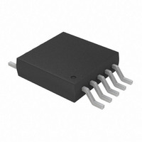
MCP4662-103E/UN Microchip Technology, MCP4662-103E/UN Datasheet - Page 16

MCP4662-103E/UN
Manufacturer Part Number
MCP4662-103E/UN
Description
IC DGTL POT 10K 256TAPS 10-MSOP
Manufacturer
Microchip Technology
Datasheet
1.MCP4541T-502EMF.pdf
(92 pages)
Specifications of MCP4662-103E/UN
Taps
257
Resistance (ohms)
10K
Number Of Circuits
2
Temperature Coefficient
150 ppm/°C Typical
Memory Type
Non-Volatile
Interface
I²C, 2-Wire Serial
Voltage - Supply
2.7 V ~ 5.5 V
Operating Temperature
-40°C ~ 125°C
Mounting Type
Surface Mount
Package / Case
10-MSOP, Micro10™, 10-uMAX, 10-uSOP
Resistance In Ohms
10K
End To End Resistance
100kohm
Track Taper
Linear
Resistance Tolerance
± 20%
No. Of Steps
256
Supply Voltage Range
2.7V To 5.5V
Control Interface
I2C, Serial
No. Of Pots
Dual
Lead Free Status / RoHS Status
Lead free / RoHS Compliant
Available stocks
Company
Part Number
Manufacturer
Quantity
Price
Company:
Part Number:
MCP4662-103E/UN
Manufacturer:
Microchip
Quantity:
229
MCP454X/456X/464X/466X
TABLE 1-2:
DS22107A-page 16
I
Note 1:
2
Param.
C AC Characteristics
No.
107
109
110
2:
3:
4:
5:
6:
7:
As a transmitter, the device must provide this internal minimum delay time to bridge the undefined region
(minimum 300 ns) of the falling edge of SCL to avoid unintended generation of START or STOP conditions.
A fast-mode (400 kHz) I
requirement t
stretch the LOW period of the SCL signal. If such a device does stretch the LOW period of the SCL signal,
it must output the next data bit to the SDA line
T
the SCL line is released.
The MCP46X1/MCP46X2 device must provide a data hold time to bridge the undefined part between V
and V
must be tested in order to ensure that the output data will meet the setup and hold specifications for the
receiving device.
Use Cb in pF for the calculations.
Not Tested
A Master Transmitter must provide a delay to ensure that difference between SDA and SCL fall times do
not unintentionally create a Start or Stop condition.
Ensured by the T
R
T
SU:DAT
T
Sym
max.+t
T
T
BUF
AA
SP
IL
I
2
of the falling edge of the SCL signal. This specification is not a part of the I
C BUS DATA REQUIREMENTS (SLAVE MODE) (CONTINUED)
SU;DAT
Characteristic
Bus free time
Input filter spike
suppression
(SDA and SCL)
Data input setup
SU;DAT
Output valid
from clock
AA
= 1000 + 250 = 1250 ns (according to the standard-mode I
time
3.4 MHz specification test.
≥ 250 ns must then be met. This will automatically be the case if the device does not
2
C-bus device can be used in a standard-mode (100 kHz) I
Standard Operating Conditions (unless otherwise specified)
Operating Temperature
Operating Voltage V
100 kHz mode
400 kHz mode
1.7 MHz mode
3.4 MHz mode
100 kHz mode
400 kHz mode
1.7 MHz mode
3.4 MHz mode
100 kHz mode
400 kHz mode
1.7 MHz mode
3.4 MHz mode
100 kHz mode
400 kHz mode
1.7 MHz mode
3.4 MHz mode
DD
4700
1300
N.A.
N.A.
range is described in
Min
250
100
10
10
—
—
—
—
—
—
—
—
—
–40°C ≤ T
3450
Max
900
150
310
150
50
50
10
10
—
—
—
—
—
—
—
—
A
≤ +125°C (Extended)
Units
ns
ns
ns
ns
ns
ns
ns
ns
ns
ns
ns
ns
ns
ns
ns
ns
ns
AC/DC characteristics
© 2008 Microchip Technology Inc.
2
C bus specification) before
Cb = 100 pF,
Time the bus must be free
Spike suppression
Spike suppression
Note 2
Note 1
Note 1, Note 7
Cb = 400 pF,
Note 1, Note 5
Cb = 100 pF, Note 1
before a new transmission
can start
Philips Spec states N.A.
2
2
C specification, but
C-bus system, but the
Conditions
IH


