MCP4662-103E/UN Microchip Technology, MCP4662-103E/UN Datasheet - Page 48
MCP4662-103E/UN
Manufacturer Part Number
MCP4662-103E/UN
Description
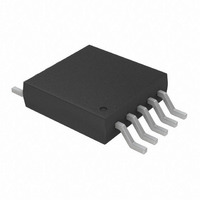
IC DGTL POT 10K 256TAPS 10-MSOP
Manufacturer
Microchip Technology
Datasheet
1.MCP4541T-502EMF.pdf
(92 pages)
Specifications of MCP4662-103E/UN
Taps
257
Resistance (ohms)
10K
Number Of Circuits
2
Temperature Coefficient
150 ppm/°C Typical
Memory Type
Non-Volatile
Interface
I²C, 2-Wire Serial
Voltage - Supply
2.7 V ~ 5.5 V
Operating Temperature
-40°C ~ 125°C
Mounting Type
Surface Mount
Package / Case
10-MSOP, Micro10™, 10-uMAX, 10-uSOP
Resistance In Ohms
10K
End To End Resistance
100kohm
Track Taper
Linear
Resistance Tolerance
± 20%
No. Of Steps
256
Supply Voltage Range
2.7V To 5.5V
Control Interface
I2C, Serial
No. Of Pots
Dual
Lead Free Status / RoHS Status
Lead free / RoHS Compliant
Available stocks
Company
Part Number
Manufacturer
Quantity
Price
Company:

Part Number:
MCP4662-103E/UN
Manufacturer:
Microchip
Quantity:
229


MCP454X/456X/464X/466X
6.2
The MCP45XX/46XX’s I
the Philips I
the modules features:
• 7-bit slave addressing
• Supports three clock rate modes:
• Support Multi-Master Applications
• General call addressing
• Internal weak pull-ups on interface signals
The I
The Philips I
types, field lengths, timings, etc. of a frame. The frame
content defines the behavior of the device. The frame
content for the MCP4XXX is defined in Section 7.0.
6.2.1
Figure 6-8
clock is generated by the master. The following defini-
tions are used for the bit states:
• Start bit (S)
• Data bit
• Acknowledge (A) bit (driven low) /
• Repeated Start bit (Sr)
• Stop bit (P)
6.2.1.1
The Start bit (see
a data transfer sequence. The Start bit is defined as the
SDA signal falling when the SCL signal is “High”.
FIGURE 6-2:
6.2.1.2
The SDA signal may change state while the SCL signal
is Low. While the SCL signal is High, the SDA signal
MUST be stable (see
FIGURE 6-3:
DS22107A-page 48
SDA
SCL
SDA
SCL
- Standard mode, clock rates up to 100 kHz
- Fast mode, clock rates up to 400 kHz
- High-speed mode (HS mode), clock rates up
No Acknowledge (A) bit (not driven low)
to 3.4 MHz
2
C 10-bit addressing mode is not supported.
I
2
S
shows the I
C Operation
2
I
C specification. The following lists some of
2
C BIT STATES AND SEQUENCE
Start Bit
Data Bit
2
C specification only defines the field
Figure
Figure
2
Start Bit.
Data Bit.
C transfer sequence. The serial
6-2) indicates the beginning of
2
C module is compatible with
1st Bit
6-5).
Data Bit
1st Bit
2nd Bit
2nd Bit
6.2.1.3
The A bit (see
the receiving device to the transmitting device.
Depending on the context of the transfer sequence, the
A bit may indicate different things. Typically the Slave
device will supply an A response after the Start bit and
8 “data” bits have been received. an A bit has the SDA
signal low.
FIGURE 6-4:
Not A (A) Response
The A bit has the SDA signal high.
some of the conditions where the Slave Device will
issue a Not A (A).
If an error condition occurs (such as an A instead of A),
then an START bit must be issued to reset the
command state machine.
TABLE 6-1:
General Call
Slave Address
valid
Slave Address
not valid
Device Mem-
ory Address
and specified
command
(AD3:AD0 and
C1:C0) are an
invalid combi-
nation
Communica-
tion during
EEPROM write
cycle
Bus Collision
SDA
SCL
Event
Acknowledge (A) Bit
Figure
8
D0
MCP45XX/MCP46XX A / A
RESPONSES
Acknowledge
Response
6-4) is typically a response from
Acknowledge Waveform.
N.A.
© 2008 Microchip Technology Inc.
Bit
A
A
A
A
A
Only if GCEN bit is
set
After device has
received address
and command
After device has
received address
and command,
and valid condi-
tions for EEPROM
write
I
Resets, or a “Don’t
Care” if the colli-
sion occurs on the
Masters “Start bit”.
2
C Module
Table 6-1
Comment
9
A
shows
Related parts for MCP4662-103E/UN
Image
Part Number
Description
Manufacturer
Datasheet
Request
R

Part Number:
Description:
IC DGTL POT 50K 256TAPS 10-MSOP
Manufacturer:
Microchip Technology
Datasheet:
Part Number:
Description:
IC DGTL POT 100K 256TAPS 10-MSOP
Manufacturer:
Microchip Technology
Datasheet:
Part Number:
Description:
IC DGTL POT 5K 256TAPS 10-MSOP
Manufacturer:
Microchip Technology
Datasheet:

Part Number:
Description:
Manufacturer:
Microchip Technology Inc.
Datasheet:
Part Number:
Description:
Manufacturer:
Microchip Technology Inc.
Datasheet:
Part Number:
Description:
Manufacturer:
Microchip Technology Inc.
Datasheet:
Part Number:
Description:
Manufacturer:
Microchip Technology Inc.
Datasheet:
Part Number:
Description:
Manufacturer:
Microchip Technology Inc.
Datasheet:
Part Number:
Description:
Manufacturer:
Microchip Technology Inc.
Datasheet:
Part Number:
Description:
Manufacturer:
Microchip Technology Inc.
Datasheet: