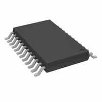
AD5204BRUZ10 Analog Devices Inc, AD5204BRUZ10 Datasheet - Page 7

AD5204BRUZ10
Manufacturer Part Number
AD5204BRUZ10
Description
IC POT DGTL QUAD 256POS 24TSSOP
Manufacturer
Analog Devices Inc
Datasheet
1.AD5204BRUZ50.pdf
(20 pages)
Specifications of AD5204BRUZ10
Taps
256
Resistance (ohms)
10K
Number Of Circuits
4
Temperature Coefficient
700 ppm/°C Typical
Memory Type
Volatile
Interface
SPI, 3-Wire Serial
Voltage - Supply
2.7 V ~ 5.5 V, ±2.3 V ~ 2.7 V
Operating Temperature
-40°C ~ 85°C
Mounting Type
Surface Mount
Package / Case
24-TSSOP
Resistance In Ohms
10K
End To End Resistance
10kohm
Track Taper
Linear
No. Of Steps
256
Resistance Tolerance
± 30%
Supply Voltage Range
2.7V To 5.5V, ± 2.3V To ± 2.7V
Control Interface
3 Wire, Serial
Lead Free Status / RoHS Status
Lead free / RoHS Compliant
Available stocks
Company
Part Number
Manufacturer
Quantity
Price
Company:
Part Number:
AD5204BRUZ10
Manufacturer:
Analog Devices Inc
Quantity:
135
Part Number:
AD5204BRUZ10
Manufacturer:
ADI/亚德诺
Quantity:
20 000
Part Number:
AD5204BRUZ10-REEL7
Manufacturer:
ADI/亚德诺
Quantity:
20 000
Company:
Part Number:
AD5204BRUZ100
Manufacturer:
ADI
Quantity:
556
Part Number:
AD5204BRUZ100
Manufacturer:
ADI/亚德诺
Quantity:
20 000
PIN CONFIGURATIONS AND FUNCTION DESCRIPTIONS
Table 3. AD5204 SOIC/TSSOP/PDIP Pin Function Descriptions
Pin No.
1, 2, 12
3
4
5
6
7
8
9
10
11
13
14
15
16
17
18
19
20
21
22
23
24
Name
NC
GND
CS
PR
V
SHDN
SDI
CLK
SDO
V
B3
W3
A3
B1
W1
A1
A2
W2
B2
A4
W4
B4
DD
SS
Description
Not Connected.
Ground.
Chip Select Input (Active Low). When CS returns high, data in the serial input register is decoded based on the address
bits, and then it is loaded into the target RDAC latch.
Preset to Midscale (Active Low). This pin sets the RDAC registers to 0x80.
Positive Power Supply. This pin is specified for operation at both 3 V and 5 V. It is the sum of |V
Terminal A Open-Circuit Shutdown (Active Low Input). This pin controls VR 1 through VR 4.
Serial Data Input. Data is input MSB first.
Serial Clock Input. This pin is positive edge triggered.
Serial Data Output. This pin is an open-drain transistor and requires a pull-up resistor.
Negative Power Supply. This pin is specified for operation at both 0 V and −2.7 V. It is the sum of |V
Terminal B RDAC 3.
Wiper RDAC 3. Address = 010
Terminal A RDAC 3.
Terminal B RDAC 1.
Wiper RDAC 1. Address = 000
Terminal A RDAC 1.
Terminal A RDAC 2.
Wiper RDAC 2. Address = 001
Terminal B RDAC 2.
Terminal A RDAC 4.
Wiper RDAC 4. Address = 011
Terminal B RDAC 4.
Figure 6. AD5204 SOIC/TSSOP/PDIP Pin Configuration
2
2
2
2
.
.
.
.
SHDN
GND
SDO
CLK
V
V
SDI
NC
NC
NC
CS
PR
DD
SS
10
12
11
1
2
3
4
5
6
7
8
9
Rev. C | Page 7 of 20
NC = NO CONNECT
(Not to Scale)
AD5204
TOP VIEW
24
23
22
21
20
19
18
17
16
15
14
13
B4
W4
A4
B2
W2
A2
A1
W1
B1
A3
W3
B3
AD5204/AD5206
DD
| + |V
DD
| + |V
SS
| < 5.5 V.
SS
| < 5.5 V.


